Semiconductor device saving data in non-volatile manner during standby

a technology of semiconductor devices and data, applied in the field of semiconductor devices, can solve the problems of data loss, data of flip-flops within logic circuits or volatile memory, and increase in leak current between source and drain of transistors in off-state, so as to achieve rapid data saving, data can be saved, and current consumption during standby is reduced

Inactive Publication Date: 2005-09-08
RENESAS TECH CORP
View PDF7 Cites 34 Cited by
  • Summary
  • Abstract
  • Description
  • Claims
  • Application Information

AI Technical Summary

Benefits of technology

[0015] Therefore, a main advantage of the present invention is that, data can be saved without interrupting a normal operation by providing a transfer path for transferring data during data saving separately from a normal data transfer path, and current consumption during standby is reduced by changing a power supply potential from a normal operation potential to a standby potential.
[0016] Another advantage of the present invention is that, as the thin film magnetic memory cell is added to the volatile latch circuit, data can rapidly be saved without requiring a complex transfer operation when data of the latch circuit is to be saved, and current consumption during standby can efficiently be reduced by changing the power supply potential to the standby potential in the standby mode.

Problems solved by technology

With such a thinner gate oxide film, a gate leak current further increases.
Reduction of the gate length also causes an increase in a leak current between source and drain of the transistor in an off-state.
When the power supply voltage is turned off, however, data of a flip-flop within a logic circuit or a volatile memory will be lost.
Because of this very long time period, much processing time is required before the power supply voltage is turned off.
As a result, a transition time to a standby mode for reducing current consumption will be late.
In addition, as the flash EEPROM also takes a relatively long time to read data, a long time period is needed to read data and return the data of the volatile memory or flip-flop to its original state after the power is reset.
Thus, it also takes a long time to activate the device.
Further, it is uneconomical to provide a memory for temporary saving on an external printed-circuit board, because the number of elements in the whole system as well as an area of the external printed-circuit board increase.

Method used


Image

  • Semiconductor device saving data in non-volatile manner during standby
  • Semiconductor device saving data in non-volatile manner during standby
  • Semiconductor device saving data in non-volatile manner during standby

Examples


first embodiment

[0039] [First Embodiment]

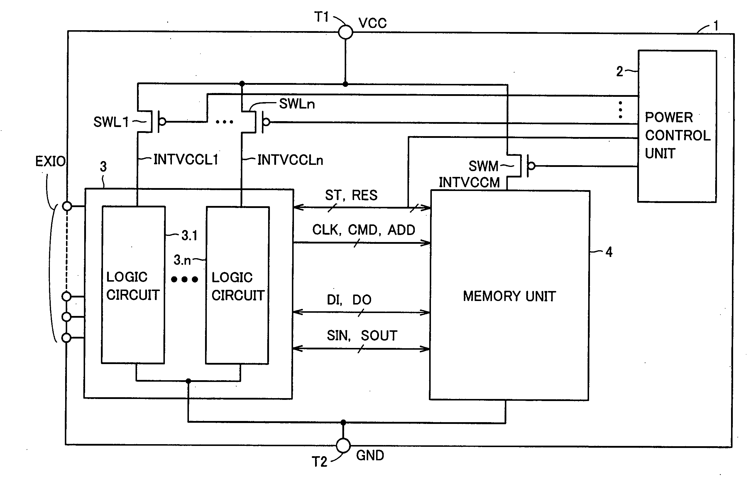
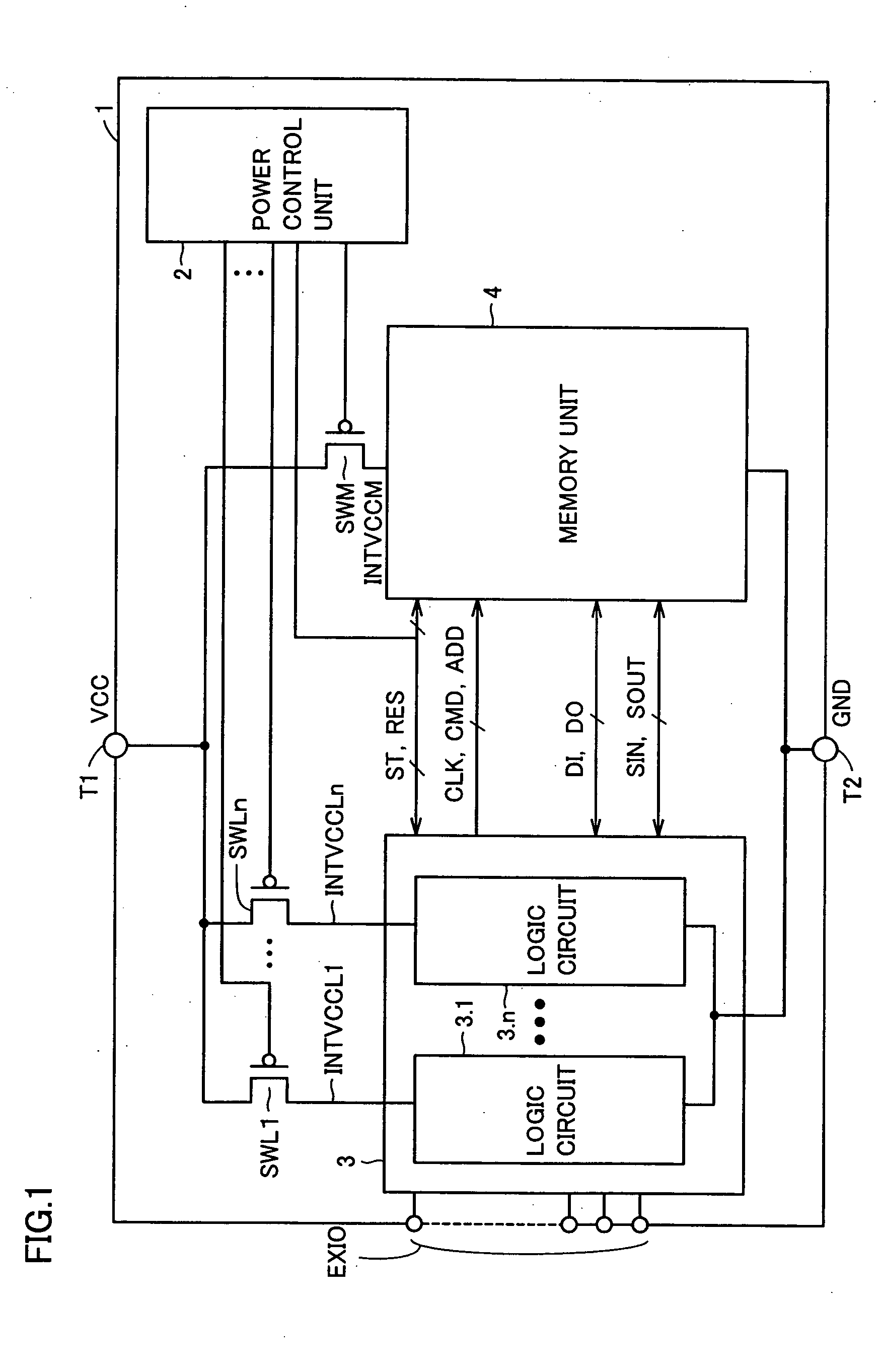
[0040]FIG. 1 is a schematic block diagram of a whole structure relating to a power control operation of a semiconductor device 1 of a first embodiment 1 according to the present invention.

[0041] Referring to FIG. 1, semiconductor device 1 includes a power supply terminal T1 receiving a power supply potential VCC fed from the outside, a ground terminal T2 receiving a ground potential GND fed from the outside, and a terminal EXIO for communicating signals with the outside.

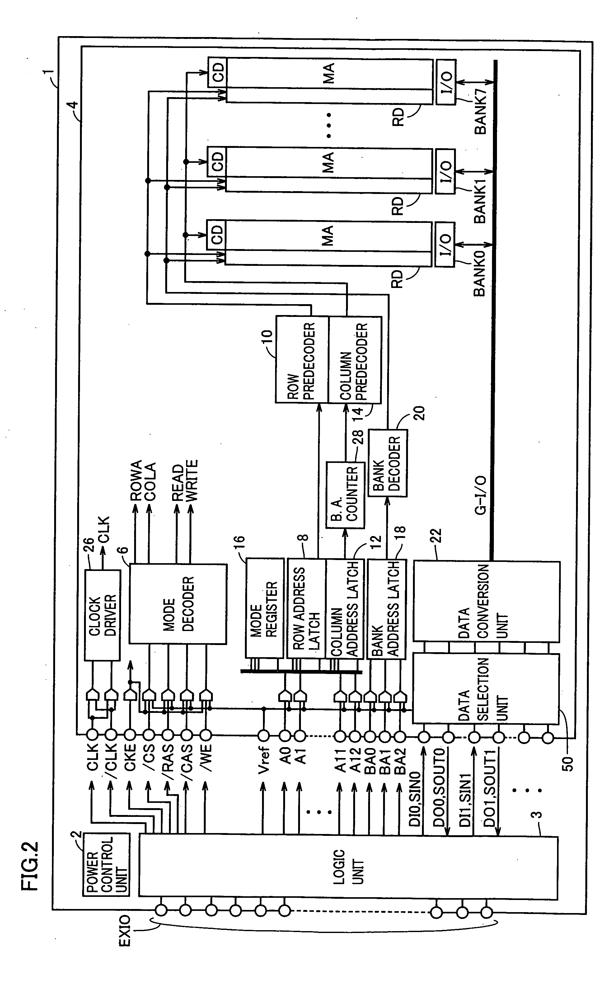
[0042] Semiconductor device 1 further includes a logic unit 3, a memory unit 4, switch circuits SWL1-SWLn and SWM, and a power control unit 2.

[0043] Logic unit 3 includes logic circuits 3.1-3.n. As will be described below, logic circuits 3.1-3.n include a circuit such as a flip-flop for temporarily storing data and a combinational circuit such as an AND circuit.

[0044] Power control unit 2 performs on / off controls of switch circuits SWL1-SWLn and SWM, and also outputs control signals ST, R...

second embodiment

[0126] [Second Embodiment]

[0127] A system LSI is formed with a plurality of circuit blocks, and a degree of integration thereof is increasing in recent years as a transistor becomes smaller. On the other hand, a decrease in a transistor threshold voltage due to a decrease in an operation voltage causes an increased leak current of the transistor. In addition, as a gate oxide film of the transistor becomes thinner, a leak current of the gate oxide film increases. Furthermore, a parasitic PN diode is formed between a source / drain and a substrate of the transistor. A reverse bias is usually applied to the PN diode. As the size thereof is reduced, a concentration of an impurity of the source / drain of the transistor increases, and a leak current of the PN diode at the application of reverse bias increases.

[0128] The three problems of the leak current described above result in an increased current during standby for the whole system LSI. In a second embodiment; another structure to decre...


PUM


Abstract

A power control unit activates a control signal ST for a circuit block to be set to a standby state before turning off power of the circuit block or a whole chip, and saves an operation result of data processing of the circuit block into a memory unit. When the power is again supplied to the circuit block in the standby state, the power control unit activates a control signal RES after the power supply is started and restores the data saved in the memory unit to the circuit block. Flip-flops in the circuit block are connected in series when the saving or restoring of data is performed, and perform a data transfer operation with a path different from that in a normal operation. Therefore, a semiconductor device can be provided which can rapidly transit to a standby mode having reduced current consumption while holding internal information.

Description

BACKGROUND OF THE INVENTION [0001] 1. Field of the Invention [0002] The present invention relates to a semiconductor device and, more specifically, to a semiconductor device which can save processed data in an integrated thin film magnetic memory element when power is turned off. [0003] 2. Description of the Background Art [0004] In recent years, large-scale circuits can be integrated in a semiconductor device, and a system LSI (large-scale integrated circuit), in which a logic circuit and a bulk memory is integrated on one chip, has been developed. In such a system LSI, a logic circuit unit and a memory unit transmit and receive information such as address, command and data via a prescribed port. [0005] With the objective of attaining higher performance, a gate oxide film of a transistor has been made thinner, and a gate length of a transistor has been reduced. With such a thinner gate oxide film, a gate leak current further increases. Reduction of the gate length also causes an in...

Claims


Application Information

Patent Timeline
Patent Type & Authority Applications(United States)
IPC IPC(8): G11C14/00G11C11/15
CPCG11C14/0081
Inventor OOISHI, TSUKASA
Owner RENESAS TECH CORP
Why Eureka
Try Eureka