Electron beam apparatus with detailed observation function and sample inspecting and observing method using electron beam apparatus

a technology of electron beam and detailed observation, which is applied in the direction of material analysis using wave/particle radiation, instruments, and therapy, etc., can solve the problems of increased inspection time and extended floor area in a clean room, and achieve the improvement of product yield, avoid shipping defective products, and high throughput

Active Publication Date: 2005-09-15
KIOXIA CORP +1
View PDF3 Cites 28 Cited by
  • Summary
  • Abstract
  • Description
  • Claims
  • Application Information

AI Technical Summary

Benefits of technology

[0007] Another object to be achieved by the present invention is to provide a sample observing method allowing for simultaneous defect coordinate extraction and detailed observation to be performed in real time and in parallel correspondence with the sample inspection, to thereby reduce the inspection time.
[0028] Further, the application of a sample observing method according to the present invention to the inspection process of a semiconductor device allows for the inspection with high throughput to be achieved even for a semiconductor device having fine pattern. Thus 100% inspection, improvement in yield of products as well as avoidance of shipping any defective products can be successfully achieved.

Problems solved by technology

Thus, in the prior art relying on the use of a separate unit such as an SEM review unit for the detailed observation, inherently a time period is required to transfer the wafer to said separate unit, which is a critical factor leading to increased inspection time.
Further, since two units, the electron beam apparatus plus the SEM review unit, are both necessary, problematically a floor area in a clean room must be extended.

Method used


Image

  • Electron beam apparatus with detailed observation function and sample inspecting and observing method using electron beam apparatus
  • Electron beam apparatus with detailed observation function and sample inspecting and observing method using electron beam apparatus
  • Electron beam apparatus with detailed observation function and sample inspecting and observing method using electron beam apparatus

Examples


example 1

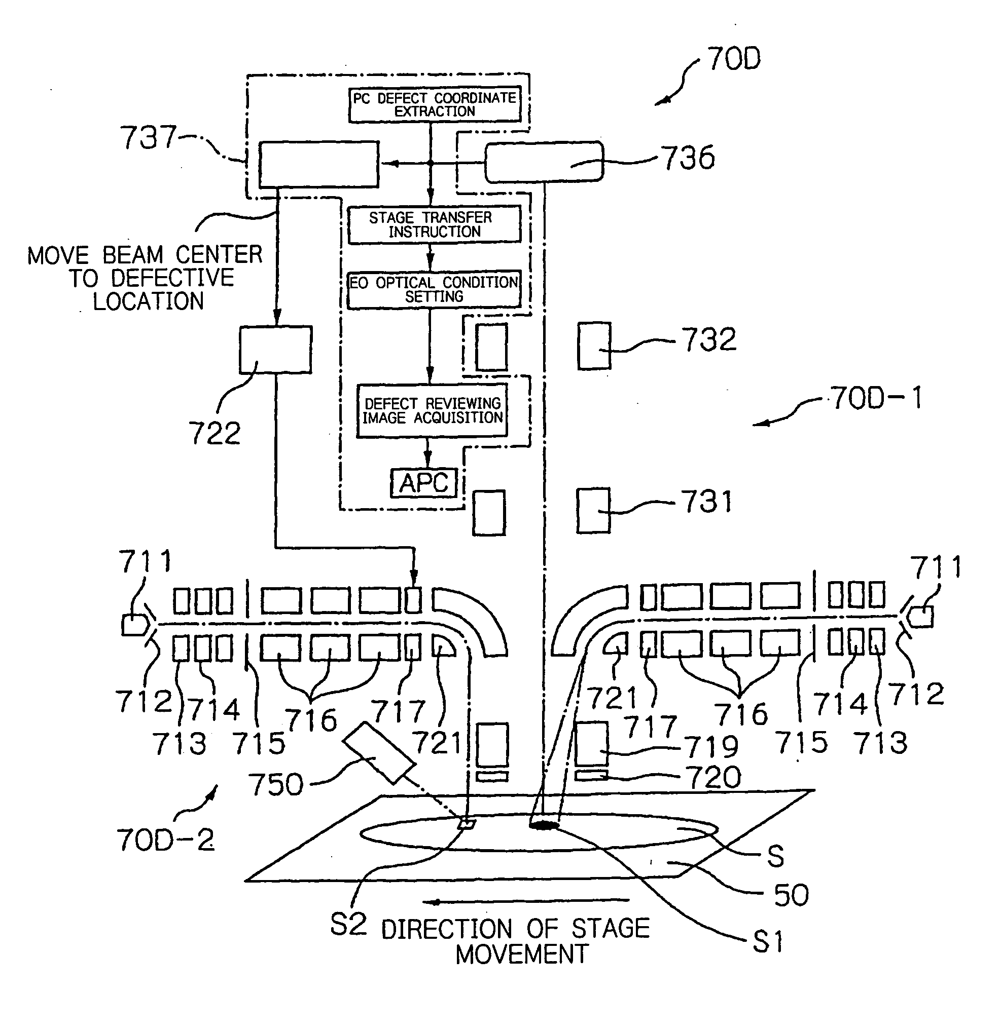
[0110]FIG. 7 schematically shows an electron beam apparatus 70 of image projection type with a single beam in example 1 of the electron beam apparatus 70 of FIG. 1. This electron beam apparatus 70 comprises a primary optical system 710 for shaping an electron ray emitted from an electron gun into a specified shape in section view and irradiating thus shaped electron beam onto a surface of a sample to be inspected, for example, a surface of a wafer S and a secondary optical system 730 for focusing secondary electrons emanating from the wafer S into an image on a detector.

[0111] The primary optical system 710 comprises a cathode 712 for drawing an electron ray from an electron source 711, an anode 713 for accelerating the electron ray (the electron source 711, the cathode 712 and the anode 713 together constructing an electron gun), an electrostatic lens 714, an aperture 715 for shaping the electron ray into an electron beam of specified shape in section view, a quadrupole lens 716 f...

example 2

[0121]FIG. 8 schematically shows an electron beam apparatus 70A of image projection type with a single beam in example 2 of the electron beam apparatus 70 of FIG. 1. This electron beam apparatus 70A has the same configuration as the electron beam apparatus in example 1 (FIG. 7), with the exceptions that a primary optical system 710A is arranged in parallel correspondence to the wafer and provided with a sector deflector 721 and that a secondary optical system 730A includes no E×B separator. In the present example, to irradiate the electron beam to a sample surface from the oblique direction relative thereto, firstly the electron beam is guided in a direction parallel to the wafer, and after passing through the aligner 717, the electron beam is controlled by the sector deflector 721 to irradiate from the oblique direction.

[0122] The manner of executing the image inspection of the wafer, the extraction of the defective region and the detailed image observation in the acquired defecti...

example 3

[0123]FIG. 9 schematically shows an electron beam apparatus 70B of image projection type with a multi-beam in example 3 of the electron beam apparatus 70 of FIG. 1. This electron beam apparatus 70B has the same configuration as the electron beam apparatus 70A in example 2, with the exception that the electron beam apparatus 70B comprises a plurality of primary optical systems 710A. Since this electron beam apparatus 70B allows for a plurality of electron beams to be irradiated on the wafer, for the observation in the low reflected electron mode defining a lower emission ratio of the electrons from the wafer, some of the total number of electron beams (e.g., three of four electron beams) may be concurrently irradiated to the same inspection region to thereby improve the S / N ratio. Further, for the case of the detailed observation to be subsequently executed, the optical condition for the rest of the electron beams (i.e., the remaining one beam of the four electron beams) may be limit...


PUM

PropertyMeasurementUnit
widthaaaaaaaaaa
diameteraaaaaaaaaa
diameteraaaaaaaaaa

Abstract

Provided is a sample observing method allowing for a detailed observation of a sample by using one and the same electron beam apparatus. The method uses an electron beam apparatus 1 comprising a primary optical system 10 serving for irradiating the electron beam onto the sample surface and a secondary optical system 30 serving for detecting secondary electrons emanating from said sample surface to form an image of the sample surface. The inspection is carried out on the sample surface, S, by irradiating the electron beam to the sample surface, and after the extraction of a defective region in the sample based on the inspection, the extracted defective region is once again applied with the irradiation of the electron beam so as to provide a magnification or a detailed observation of the defective region.

Description

BACKGROUND OF THE INVENTION [0001] The present invention relates to a sample observing method for inspecting, observing or evaluating features and electric continuity (electron beam testing) on a sample surface by using an electron beam apparatus, and also to a manufacturing method for fabricating a device by using said sample observing method; and more specifically relates to an inspecting method for inspecting a sample (e.g., a wafer) having a device pattern with a minimum line width equal to or smaller than 0.1 μm for defects with high throughput as well as high accuracy and high reliability, and also to a manufacturing method for fabricating a device, which allows for an improvement in yield by using said inspecting method to inspect the wafer or the like in the course of processing. [0002] There is a known technology according to the prior art, including an apparatus for detecting a defect and an inspection method employing such an apparatus, in which a defect can be detected b...

Claims


Application Information

Patent Timeline
Patent Type & Authority Applications(United States)
IPC IPC(8): G01N23/00G01R31/305G21K7/00
CPCG01R31/305
Inventor WATANABE, KENJISATAKE, TOHRUNOJI, NOBUHARUMURAKAMI, TAKESHIKARIMATA, TSUTOMUYAMAZAKI, YUICHIRONAGAHAMA, ICHIROTAONISHI, ATSUSHI
Owner KIOXIA CORP
Why Eureka
Try Eureka