High power diode utilizing secondary emission
a high-power diode and secondary emission technology, applied in the field of high-power diodes, can solve the problems of diode short circuit, diode impedance collapse, and inability to meet the requirements of high-power diodes, and achieve the effect of increasing the lifetime of the diodes
- Summary
- Abstract
- Description
- Claims
- Application Information
AI Technical Summary
Benefits of technology
Problems solved by technology
Method used
Image
Examples
Embodiment Construction
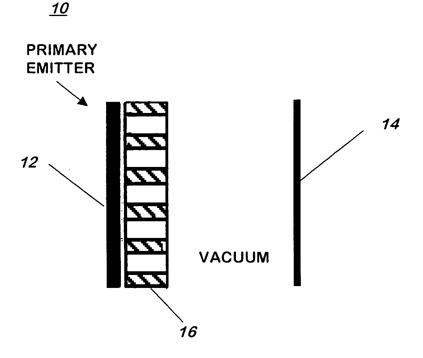
[0046] Referring now to FIG. 3a, a high power diode 10 includes a cathode 12 (the “primary emitter” as indicated), an anode 14, and a porous dielectric layer 16 spaced a selected distance from the cathode 12. Preferred cathode 12 materials include velvet, carbon fiber, and carbon cloth. Layer 16 is preferably a honeycomb ceramic as illustrated in FIG. 4.
[0047] Referring to FIG. 3a, a honeycomb slab is placed 2 mm above the emitter and supported by ceramic spacers at the edges. A suitable honeycomb material is cordierite with the bulk material dielectric constant of 6.3. The honeycomb consists of square pores with a pore size of 1.2 mm×1.2 mm with a wall thickness of about 0.2 mm. Honeycomb slabs of thickness of 2 cm and 5 cm were tested. The anode is placed about 5 cm away from the surface of the ceramic. FIG. 3b shows the axial electric field distribution across the diode for a slab 2 cm thick obtained from particle in cell (PIC) simulations (MAGIC, see above). This figure shows t...
PUM
 Abstract
Description
Claims
Application Information


