Monolithic semiconductor light source with spectral controllability

Inactive Publication Date: 2005-09-15
AHURA CORP
View PDF8 Cites 33 Cited by
  • Summary
  • Abstract
  • Description
  • Claims
  • Application Information

AI Technical Summary

Benefits of technology

[0030] More particularly, in one form of the invention, there is provided a system for amplifying optical signals comprising: an optical fiber for carrying the optical signals; a high power broadband light source; and a connector for introducing the high power broadband light source into the optical fiber as a Raman pump so as to induce Raman amplification of the optical signals within the fiber.
[0031] In another form of the invention, there is provided a method for amplifying optica

Problems solved by technology

As the optical data signal travels through the fiber, however, fiber nonlinearities, fiber loss, and amplified spontaneous emission (ASE) all act to degrade the signal-to-noise ratio of the data signal.
Extended amplifier span, however, results in high ASE accumulation from low input to amplifiers, and/or large nonlinear effects due to the use of high launch power.
Currently, OEO regeneration is responsible for a much larger percentage of overall system cost than amplifiers.
As a result, when an optical channel is added or dropped from the fiber, the gains for all of the other channels change, causing network transients, distortions and misbalances.
However, applications of Raman amplifiers in the CATV industry are currently impaired by cost.
The upper limit of realistically useful Raman gain is generally limited by the double Rayleigh scattering process.
At that upper limit, the Rayleigh back scattering causes multiple reflections of both the ASE and the signal, thus causing performance degradation of the transmission.
However, current polarization scrambling techniques are generally relatively costly and bulky, and have unproven reliability.
A

Method used


Image

  • Monolithic semiconductor light source with spectral controllability
  • Monolithic semiconductor light source with spectral controllability
  • Monolithic semiconductor light source with spectral controllability

Examples


first embodiment

6.2.2.1 First Embodiment

[0082]FIG. 10 is a schematic diagram of a semiconductor die 100 used in a first preferred embodiment. The die 100 consists of a serial connection of a wavelength seed section 103 and a power booster or power amplification section 106 formed along a semiconductor waveguide 109.

[0083] The wavelength seed section 103 preferably comprises multiple subsections 103A, 103B, 103C, etc. formed along the semiconductor waveguide 109. Three subsections 103A, 103B, 103C are shown in FIG. 10; however, it should be appreciated that this number is merely exemplary and more or less than this number of wavelength seed subsections may be used. The gain profile within each subsection 103A, 103B, 103C, etc. is chosen so as to provide ASE in a particular wavelength range. The gain profiles can be defined in each subsection 103A, 103B, 103C, etc. by such techniques as epitaxial regrowth or quantum well intermixing. The quantum well blocks of these subsections are designed to provi...

second embodiment

6.2.2.2 Second Embodiment

[0089]FIG. 11 is a schematic diagram of a semiconductor chip 200 and optical train 203 used in a second preferred embodiment. Although multiple chips can be used, this embodiment will be described in the context of a single chip 200 comprising an array of parallel waveguides 206, where the array comprises a plurality (e.g., 2 to 10) of parallel waveguides 206A, 206B, 206C, etc. The gain profile (i.e., peak wavelength and shape) of each waveguide 206A, 206B, 206C, etc. is chosen so as to provide the ASE output in a particular wavelength range (e.g., 3-30 nm).

[0090] The gain profiles can be defined within each waveguide 206A, 206B, 206C, etc. by employing such techniques as epitaxial regrowth, quantum well intermixing or other techniques known in the art. The spectral width and intensity of the ASE emitted from each waveguide 206A, 206B, 206C, etc. can be tailored through the design of the active region, the length of the waveguide, and active adjustment of t...

third embodiment

6.2.2.3 Third Embodiment

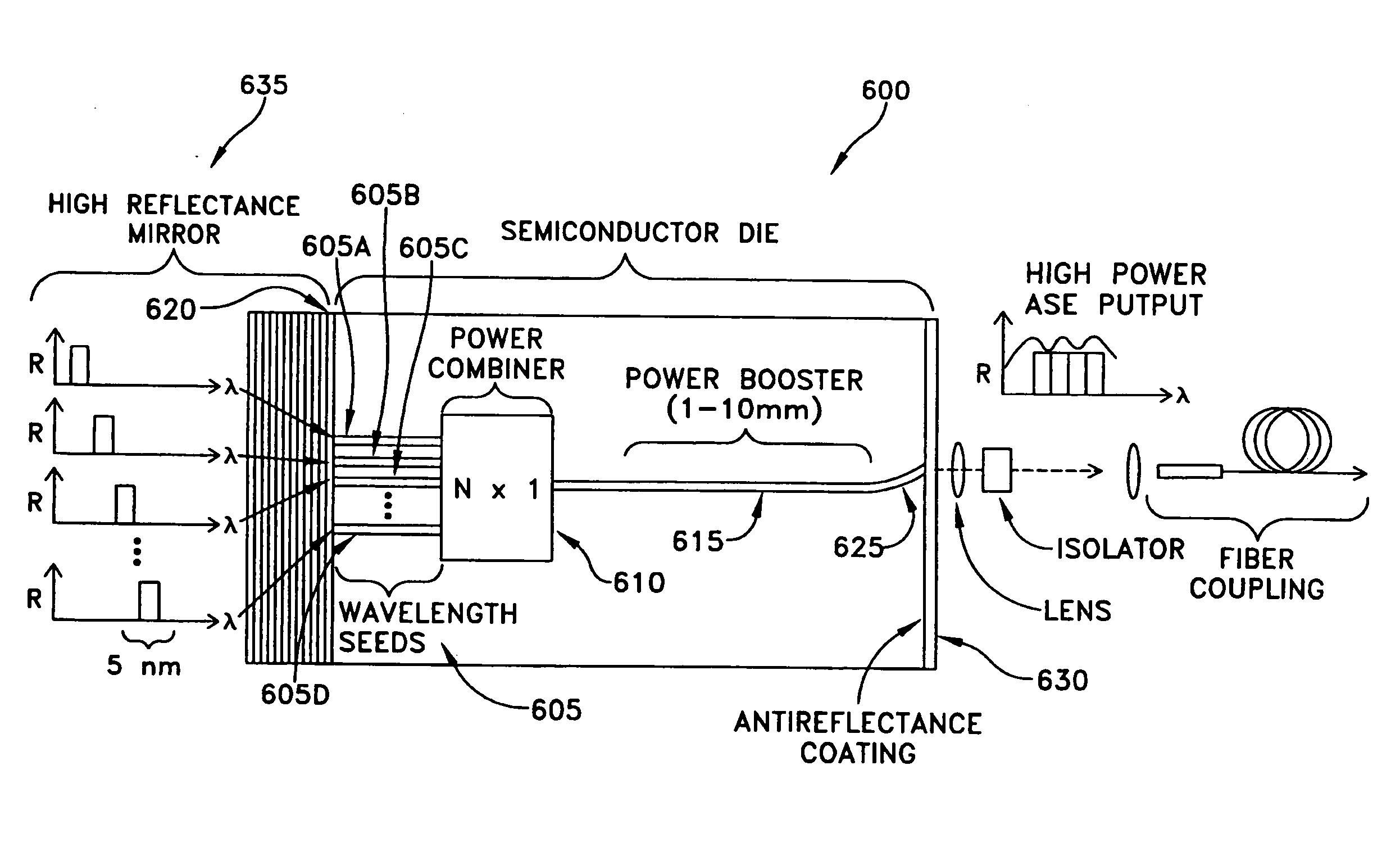
[0094]FIG. 12 is a schematic diagram of a semiconductor chip 300 and optical train 303 used in a third preferred embodiment. The die 306 consists of a wavelength seed section 309 which is power multiplexed by a multiplexer 312 into a long low loss power amplification (or booster) waveguide 315. Wavelength seed section 309 preferably comprises a plurality of wavelength seeds 309A, 309B, 309C, etc. Both the seed light waveguides 309A, 309B, 309C, etc. and the power booster waveguide 315 are designed for broadband ASE emission, just as in the first embodiment (FIG. 10) discussed above. A high reflectance mirror is provided for each of the seed waveguides 309A, 309B, 309C, etc. These mirrors may be independent of one another, or they may be different sections of a single mirror, such as is shown in FIG. 12 with the high reflectance mirror 318. The reflectivity profiles of the high reflectance mirror for each seed waveguide 309A, 309B, 309C, etc. are optimized to ...


PUM


Abstract

The invention is in the field of distributed Raman amplification for digital and analog transmission applications and other applications, e.g., instrumentation and imaging applications, including HFC-CATV applications. In particular, the invention uses a high power broadband source of amplified spontaneous emission (ASE) as the Raman pump source for improved system performance. The invention also includes methods for constructing such a high-power broadband Raman pump.

Description

1. REFERENCE TO PENDING PRIOR PATENT APPLICATION [0001] This patent application (i) claims benefit of pending prior U.S. Provisional Patent Application Ser. No. 60 / 440,115, filed Jan. 15, 2003 by Kevin Knopp et al. for MONOLITHIC SEMICONDUCTOR LIGHT SOURCE WITH SPECTRAL CONTROLLABILITY (Attorney's Docket No. AHURA-3 PROV) and (ii) is a continuation-in-part of pending U.S. patent application Ser. No. 10 / 632,779, filed Aug. 01, 2003 by Daryoosh Vakhshoori et al. for SYSTEM FOR AMPLIFYING SIGNALS (Attorney's Docket No. AHURA-1), which two patent applications are hereby incorporated herein by reference.2. FIELD OF THE INVENTION [0002] This invention relates to optical systems in general, and more particularly to systems for amplifying optical signals. 3. BACKGROUND OF THE INVENTION [0003] 3.1 In General [0004] Dense wavelength-division multiplexing (DWDM) is currently the preferred method for satisfying bandwidth demand for fiber-optic long-haul transport in telecommunication systems. A...

Claims


Application Information

Patent Timeline
IPC IPC(8): G02B6/12G02B6/42H04B10/17
CPCG02B6/12H04B10/2916G02B6/4201G02B6/4213G02B6/4215
Inventor KNOPP, KEVIN J.VAKHSHOORI, DARYOOSHWANG, PEIDONG
Owner AHURA CORP
Why Eureka
Try Eureka