Formation of ultra-shallow junctions by gas-cluster ion irradiation

a technology of gas-cluster ion irradiation and ultra-shallow junction, which is applied in the direction of basic electric elements, electrical discharge tubes, electrical apparatus, etc., can solve the problems of low processing throughput, undetected deep junctions, and difficult formation of shallowly doped semiconductors with abrupt interfaces, so as to increase the solid solubility of boron and achieve the effect of high boron doping levels and high efficiency

Active Publication Date: 2005-09-15
TEL EPION
View PDF7 Cites 58 Cited by
  • Summary
  • Abstract
  • Description
  • Claims
  • Application Information

AI Technical Summary

Benefits of technology

[0015] For some semiconductor products, an important requirement for the introduction of dopants into the semiconductor surface or for the formations of films is that the maximum depth to which the dopant has been introduced be rather shallow, on the order of several tens of angstroms to a few hundred angstroms. Gas-cluster ion beams are particularly suited for shallow doping because, while the gas-cluster ions may be accelerated to several kilo-electron volts (or even several tens of kilo-electron volts) of energy, because the clusters typically consist of thousands of atoms, individual atoms have little energy and do not ballistically penetrate the irradiated surface to great depths as occurs in conventional ion implantation and other monomer ion processes. The depth of the effects produced by energetic gas-cluster impact can be controlled by controlling the energy of the gas-cluster and, through such control, films of 100 angstroms or even less can be formed and / or processed. In addition, it is noted that gas-cluster ion beams are very efficient at infusing cluster constituents into the surfaces they irradiate. Conventional ion beams typically implant one or at most a few atoms per ion. In the case of a GCIB, the efficiency is much higher. As an example, a gas-cluster ion beam formed of clusters formed from a mixture of 5% germane in argon will typically incorporate from 100 to 2000 germanium atoms per gas-cluster ion into the irradiated surface, the exact number being controllably and repeatably dependent on beam parameters. The infused films tend to be amorphous or polycrystalline, but they can be converted to crystalline films by applying a thermal annealing step (e.g., at a temperature at or below 600 C), either a rapid anneal or a furnace anneal, preferably a non-diffusing or low-diffusing anneal. If needed to optimize anneal conditions a post-infusion-amorphization step can be done by conventional ion implantation, or by GCIB infusion of, for example, germanium by employing germanium-containing energetic gas-cluster ions. With suitable clusters containing both a dopant (boron for example) and an amorphizing agent (germanium for example) a single GCIB infusion step can produce a very shallow doped and amorphized layer that can be annealed and activated without a separate amorphizing step. When GCIB infusion of both boron and germanium is performed in a silicon substrate, the presence of the germanium can also serve to increase the solid solubility of the boron in the silicon, permitting higher boron doping levels.
[0016] Inert gas gas-cluster ion beam processing of a GCIB infusion doped semiconductor can be used to improve the depth-distribution profile of the dopant when it is desired to flatten the profile peak while yet retaining a shallow, abrupt depth-distribution tail.

Problems solved by technology

The formation of a shallowly doped semiconductor having an abrupt interface is difficult.
Typical ion implanters suffer from greatly reduced ion beam currents at very low energies and therefore result in a low processing throughput.
All these methods require a pre-amorphizing implant to prevent ion channeling of the doping implant species, which would otherwise produce undesirably deep junctions.
A pre-amorphizing implant is an ion implantation step done prior to a doping step for the purpose of damaging the region to be doped so as to reduce or eliminate the crystallinity of the region to reduce the degree of channeling of the dopant, which would otherwise result in a dopant depth distribution with an undesirably deep tail due to channeled dopant atoms.
With conventional ion beams, including even molecular ion beams (decaborane, for example) the development of high doping levels using the low beam currents available at the very low ion energies required for shallow junction doping is a low productivity process.
Additionally, the solid solubility limit of the dopant in silicon has been an upper limit for effective doping.
Consequently, the impact effects of large clusters are substantial, but are limited to a very shallow surface region.

Method used


Image

  • Formation of ultra-shallow junctions by gas-cluster ion irradiation
  • Formation of ultra-shallow junctions by gas-cluster ion irradiation
  • Formation of ultra-shallow junctions by gas-cluster ion irradiation

Examples


Embodiment Construction

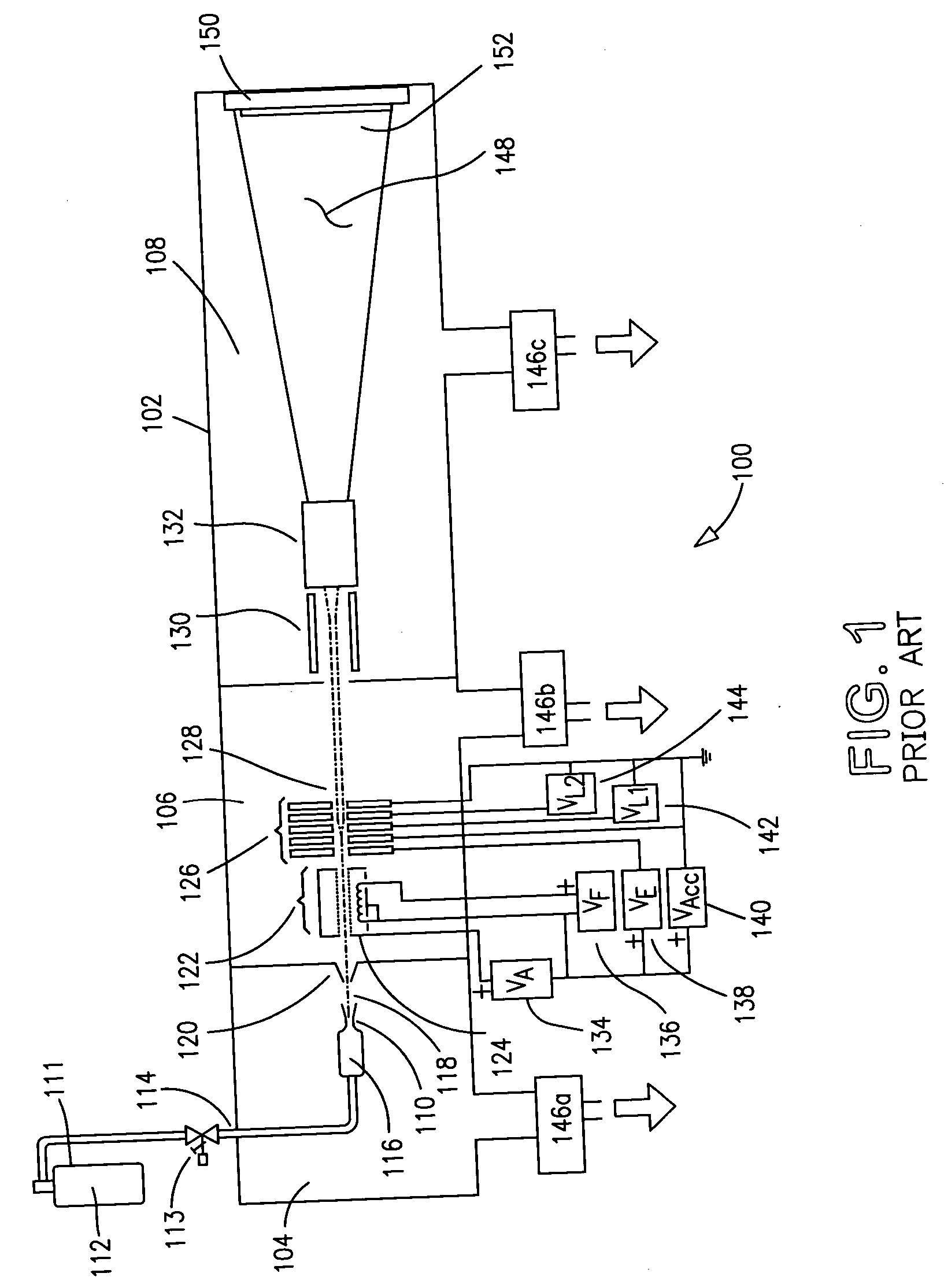
[0035]FIG. 1 shows a schematic of the basic elements of a prior art configuration for a processing apparatus 100 for generating a GCIB in accordance with the present invention. Apparatus 100 may be described as follows: a vacuum vessel 102 is divided into three communicating chambers, a source chamber 104, an ionization / acceleration chamber 106, and a processing chamber 108. The three chambers are evacuated to suitable operating pressures by vacuum pumping systems 146a, 146b, and 146c, respectively. A condensable source gas 112 (for example argon or N2) stored in a gas storage cylinder 111 is admitted under pressure through gas metering valve 113 and gas feed tube 114 into stagnation chamber 116 and is ejected into the substantially lower pressure vacuum through a properly shaped nozzle 110. A supersonic gas jet 118 results. Cooling, which results from the expansion in the jet, causes a portion of the gas jet 118 to condense into clusters, each consisting of from several to several ...


PUM


Abstract

Method of forming one or more doped regions in a semiconductor substrate and semiconductor junctions formed thereby, using gas cluster ion beams.

Description

CROSS-REFERENCE TO RELATED APPLICATIONS [0001] This application claims the benefit of priority to U.S. Provisional Patent Application Ser. No. 60 / 552,505 filed 12 Mar. 2004 entitled “Formation of Ultra-shallow Junctions by Gas-cluster Ion Irradiation,” the contents of which are hereby incorporated by reference.FIELD OF THE INVENTION [0002] This invention relates generally to the doping and activation of semiconductor substrates. More particularly, it relates to the formation of ultra-shallow semiconductor junctions by energetic gas-cluster ion irradiation. BACKGROUND OF THE INVENTION [0003] The characteristics of semiconductor materials such as silicon, germanium and gallium arsenide and other semiconductors have been exploited to form a large variety of useful devices in the fields of electronics, communications, electro-optics, and nano-technology. Ultra shallow junctions are required for future semiconductor devices. The formation of a shallowly doped semiconductor having an abru...

Claims


Application Information

Patent Timeline
Patent Type & Authority Applications(United States)
IPC IPC(8): H01L21/425
CPCH01J37/08H01J37/3171H01J2237/0812H01L21/324H01L21/265H01L21/26513H01L21/26566H01L21/223H01L21/2658
Inventor BORLAND, JOHN O.HAUTALA, JOHN J.SKINNER, WESLEY J.
Owner TEL EPION
Why Eureka
Try Eureka