Memory device and storage apparatus

a memory device and storage device technology, applied in semiconductor devices, digital storage, instruments, etc., can solve the problems of difficult to reduce the size of the device, difficult to maintain the characteristics of the above-mentioned nonvolatile memory, and increase the manufacturing cost of the dram, etc., to achieve a relatively stable reading

Inactive Publication Date: 2005-10-13
SONY CORP
View PDF9 Cites 49 Cited by
  • Summary
  • Abstract
  • Description
  • Claims
  • Application Information

AI Technical Summary

Benefits of technology

[0025] In view of the aforesaid aspect, it is an object of the present invention to provide a memor

Problems solved by technology

However, since the DRAM is complex in manufacturing process as compared with ordinary logic circuit (large scale integrated circuit (LSI circuit)) and a signal processing circuit, it is unavoidable that the manufacturing cost of the DRAM increases.
However, the above-mentioned nonvolatile memories become difficult to maintain characteristics of memory devices as the memory device comprising each memory cell is being reduced in size.
As a consequently, it is difficult to reduce the device in size up to the limit of a design rule and up to the limit of a manufacturing process.
However, the above-mentioned memory device having the structure in which any one of the upper electrode or the lower electrode contains Ag, Cu, Zn and in which the GeSe amorphous chalcogenide material is sandwiched by these electrodes encounters with the problem in which the aforementioned ion conductor whose resistance is changes is promoted to be crystallized by causes such as the rise of temperature in the manufacturing process, the rise of temperature generated by Joule heat of a recording current, a heat lo

Method used


Image

  • Memory device and storage apparatus
  • Memory device and storage apparatus
  • Memory device and storage apparatus

Examples


Embodiment Construction

[0130] The present invention will now be described in detail with reference to the drawings.

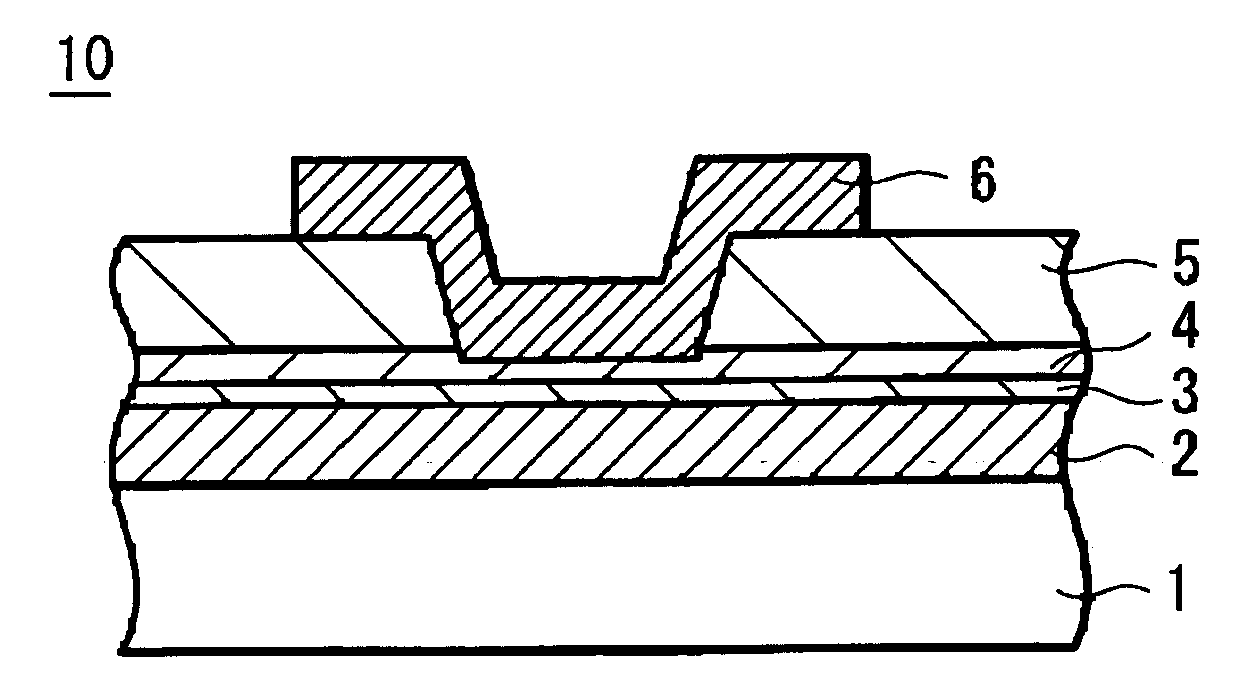
[0131]FIG. 1 of the accompanying drawings is a schematic diagram (cross-sectional view) showing an arrangement of a memory device according to an embodiment of the present invention.

[0132] As shown in FIG. 1, a memory device 10 includes a substrate 1 with a high electric conductivity, for example, a (P++) silicon substrate 1 which is heavily doped with P-type impurities and on which a lower electrode 2 is formed. This lower electrode 2 has formed thereon a layer 3 containing Cu, Ag, Zn on which a memory thin film 4 is formed. An upper electrode 6 is connected to the memory thin film 4 through a through-hole formed on an insulating layer 5 on this memory thin film 4.

[0133] The lower electrode 2 can be made of interconnection materials for use with the semiconductor process, for example, TiW, Ti, W, WN, Cu, Al, Mo, Ta, silicide and the like.

[0134] When the lower electrode 2 is made of a TiW...


PUM


Abstract

A memory device 10 has an arrangement in which a memory thin film 4 is sandwiched between first and second electrodes 2 and 6, the memory thin film 6 contains at least rare earth elements, the memory thin film 4 or a layer 3 in contact with the memory thin film 4 contains any one of elements selected from Cu, Ag, Zn and the memory thin film 4 or the layer 3 in contact with the memory thin film 4 contains any one of elements selected from Te, S, Se. The memory device can record and read information with ease stably, and this memory device can be manufactured easily by a relatively simple manufacturing method.

Description

BACKGROUND OF THE INVENTION [0001] 1. Field of the Invention: [0002] The present invention relates to a memory device capable of recording information and a storage apparatus using such a memory device. [0003] 2. Description of the Related Art: [0004] In information equipment such as computers, a high-density DRAM (dynamic RAM (random-access memory)) which can be operated at high speed is widely used as a random-access memory. [0005] However, since the DRAM is complex in manufacturing process as compared with ordinary logic circuit (large scale integrated circuit (LSI circuit)) and a signal processing circuit, it is unavoidable that the manufacturing cost of the DRAM increases. [0006] Also, the DRAM is a volatile memory of which information is lost when de-energized so that refresh operations should be made frequently, that is, written information (data) should be read out, amplified and again written in the DRAM. [0007] For this reason, a FeRAM (ferroelectric memory) and an MRAM (m...

Claims


Application Information

Patent Timeline
IPC IPC(8): H01L27/105G11C11/00G11C13/02H01L21/105H01L21/8247H01L27/10H01L27/115H01L27/24H01L45/00
CPCG11C13/0007H01L45/1625G11C2213/11G11C2213/15G11C2213/33G11C2213/34G11C2213/56G11C2213/72H01L27/2409H01L27/2436H01L45/085H01L45/1233H01L45/1266H01L45/143H01L45/144H01L45/145H01L45/146G11C13/0011H10B63/20H10B63/30H10N70/245H10N70/8416H10N70/8825H10N70/883H10N70/026H10N70/8828H10N70/8833H10N70/826G11C13/00H10N70/8822H10N70/046
Inventor ARATANI, KATSUHISAMAESAKA, AKIHIROKOUCHIYAMA, AKIRATSUSHIMA, TOMOHITO
Owner SONY CORP
Why Eureka
Try Eureka