High voltage double diffused drain MOS transistor with medium operation voltage

a technology of mos transistor and high voltage, which is applied in the direction of semiconductor devices, basic electric elements, electrical apparatus, etc., can solve the problems of reduced reliability, long-term device degradation, and increased electric field in the channel close to the drain, so as to achieve the effect of not degrading performance and reducing the resistance ron of the hv dddmos

Inactive Publication Date: 2005-10-13
TAIWAN SEMICON MFG CO LTD
View PDF22 Cites 57 Cited by
  • Summary
  • Abstract
  • Description
  • Claims
  • Application Information

AI Technical Summary

Benefits of technology

[0011] Advantages of preferred embodiments of the present invention include providing an HV DDDMOS structure and method of manufacture thereof, wherein one of the diffusion regions of the DDD is formed before the formation of the gate of the transistor. The second-formed diffusion region is self-aligned to the spacer adjacent the gate, resulting in a transistor that has a medium operating voltage, e.g., about 6 volts to 10 volts. The novel HV DDDMOS structure allows the transistor to be manufactured in a smaller scale, e.g., about 50% smaller than prior art HV DDDMOS transistors. Advantageously, no additional masks are required to manufacture the device. If low voltage devices or transistors are fabricated on the same integrated circuit, their performance is not degraded by the presence of the high voltage DDDMOS transistor having a medium operating voltage. Furthermore, the resistance Ron of the HV DDDMOS may be reduced.

Problems solved by technology

However, the high doping concentrations of shallow source and drain regions lead to an increase in the electric field in the channel close to the drain.
The high electric field causes electrons in the device channel to gain energy and be injected into the gate oxide, which is a phenomenon that is referred to as a “hot electron” problem.
The hot electron phenomenon leads to long term device degradation and reduced reliability.

Method used


Image

  • High voltage double diffused drain MOS transistor with medium operation voltage
  • High voltage double diffused drain MOS transistor with medium operation voltage
  • High voltage double diffused drain MOS transistor with medium operation voltage

Examples


Embodiment Construction

[0022] The making and using of the presently preferred embodiments are discussed in detail below. It should be appreciated, however, that the present invention provides many applicable inventive concepts that can be embodied in a wide variety of specific contexts. The specific embodiments discussed are merely illustrative of specific ways to make and use the invention, and do not limit the scope of the invention.

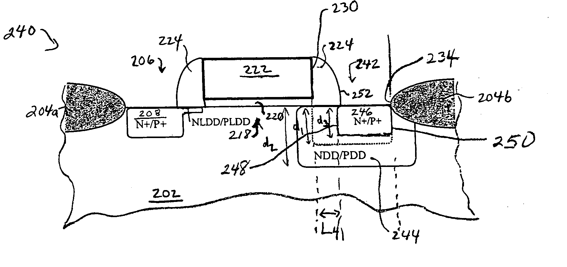
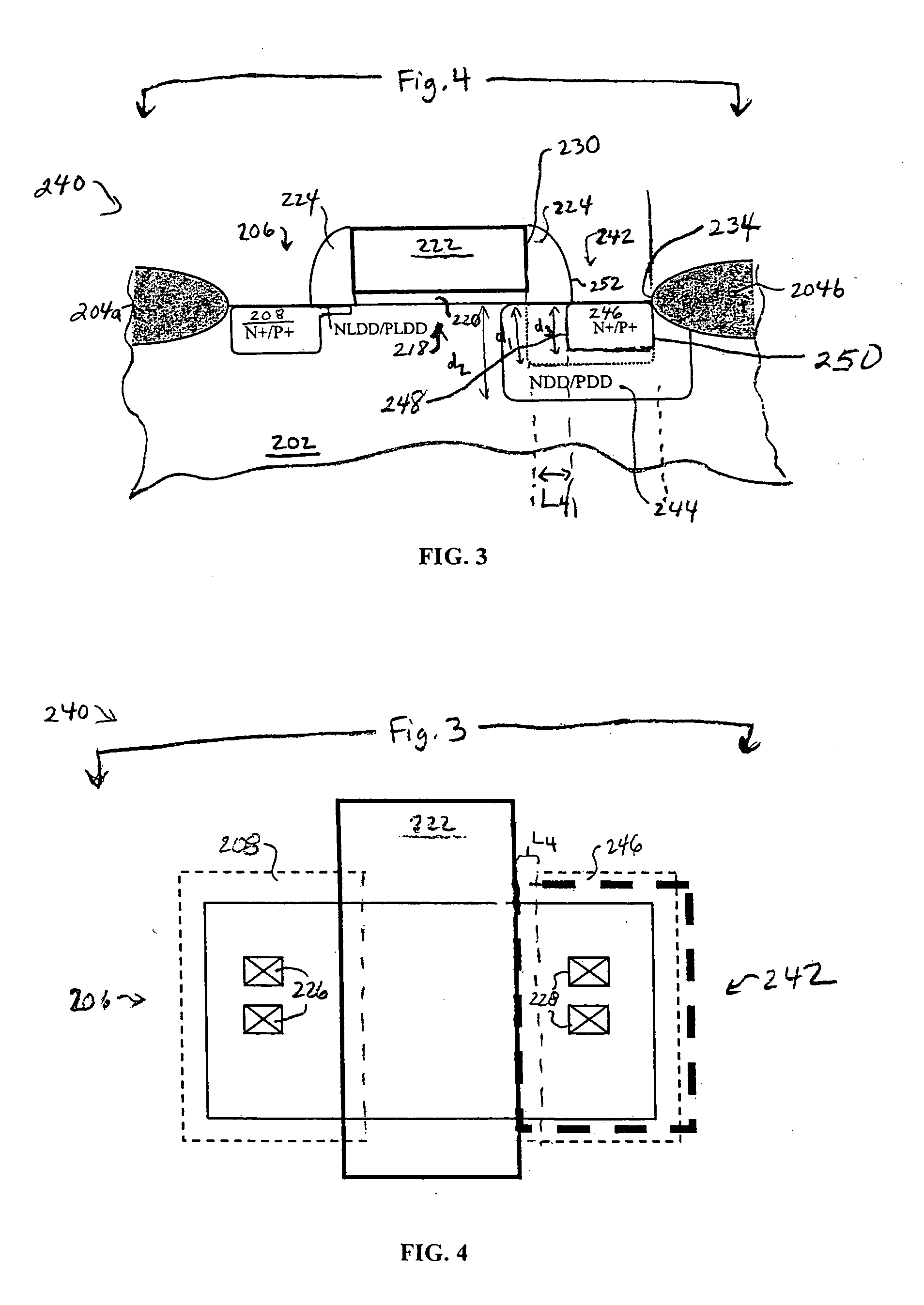
[0023] The present invention will be described with respect to preferred embodiments in a specific context, namely an HV DDDMOS device. Embodiments of the present invention may also be applied, however, to other transistor structures and methods of fabrication thereof. While only one or two transistors are shown in each figure, there may be many transistors formed simultaneously on a single semiconductor workpiece (not shown).

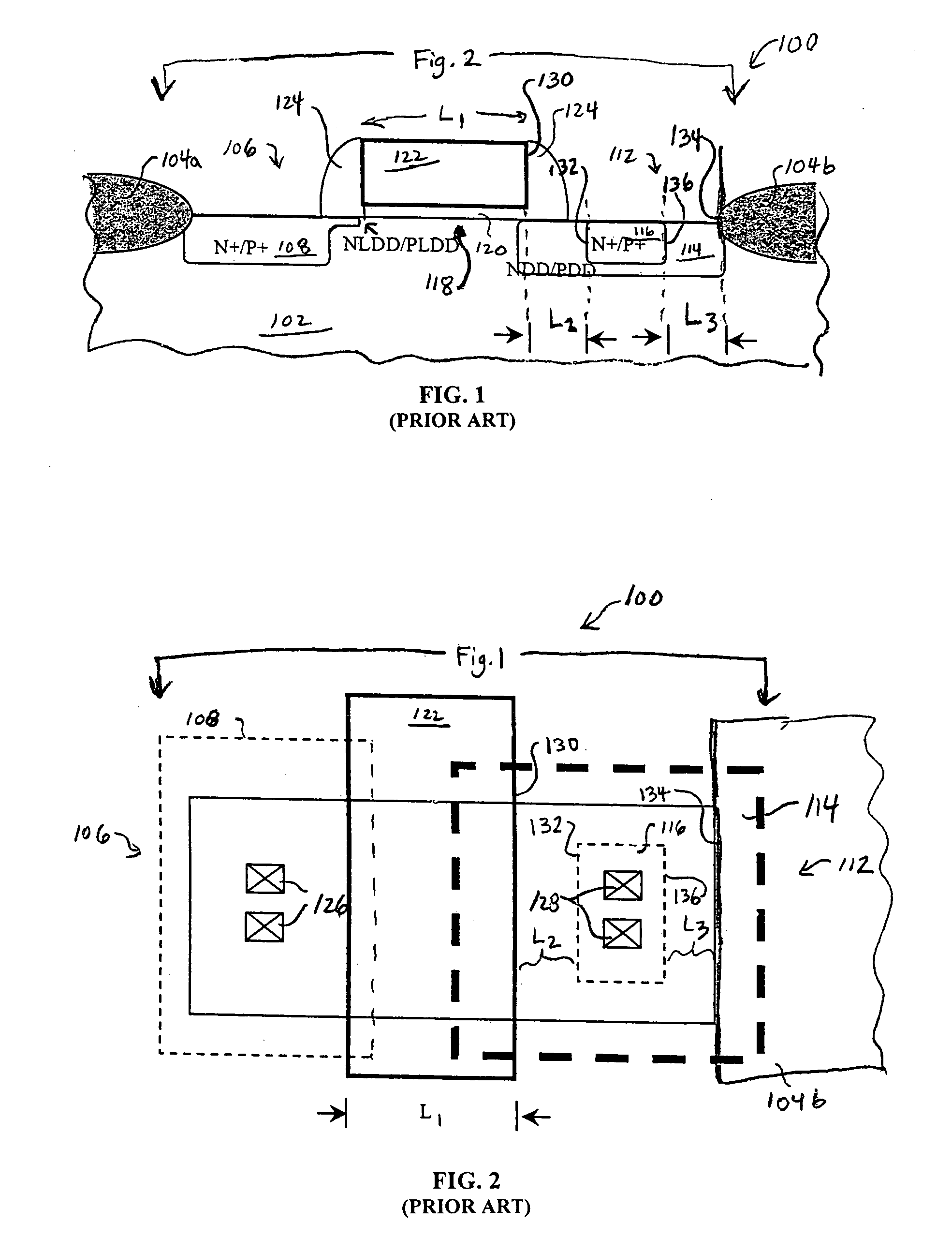
[0024] With reference now to FIG. 1, there is shown a prior art HVMOS transistor 100 which includes a workpiece 102 in which field oxide regions 104a...


PUM


Abstract

A method of fabricating a high voltage MOS transistor with a medium operation voltage on a semiconductor wafer. The transistor has a double diffused drain (DDD) and a medium operation voltage such as 6 to 10 volts, which is advantageous for applications having both low and higher operation transistor devices. The second diffusion region of the DDD is self-aligned to the spacer on the sidewalls of the gate and gate dielectric, so that the transistor size may be decreased.

Description

TECHNICAL FIELD [0001] The present invention relates generally to the fabrication of semiconductor devices, and more particularly to the fabrication of transistor devices with double diffused drains (DDD). BACKGROUND [0002] The trend in the semiconductor industry is towards reducing device dimensions. For example, in the manufacturing of highly dense integrated circuits that use metal oxide semiconductor field effect transistors (MOSFETs), as device dimensions are decreased, there is a need to create shallower source and drain regions. However, the high doping concentrations of shallow source and drain regions lead to an increase in the electric field in the channel close to the drain. The high electric field causes electrons in the device channel to gain energy and be injected into the gate oxide, which is a phenomenon that is referred to as a “hot electron” problem. The hot electron phenomenon leads to long term device degradation and reduced reliability. [0003] One approach to mi...

Claims


Application Information

Patent Timeline
Patent Type & Authority Applications(United States)
IPC IPC(8): H01L21/331H01L21/336H01L21/8222H01L21/8234H01L29/06H01L29/08H01L29/78
CPCH01L21/823418H01L29/0692H01L29/7835H01L29/66659H01L29/0847
Inventor CHEN, FU-HSINLIN, YI-CHUNLIU, RUEY-HSIN
Owner TAIWAN SEMICON MFG CO LTD
Why Eureka
Try Eureka