Memory device and method of making the same

a memory device and memory technology, applied in the field of memory and storage systems, can solve the problems of inability to adapt to the changing needs of the user, and the inability to use the device at all, so as to achieve high and low resistance levels of the memory element, easy adjustment, and high and low resistance level of the memory element

Inactive Publication Date: 2005-10-27
GLOBALFOUNDRIES US INC
View PDF20 Cites 21 Cited by
  • Summary
  • Abstract
  • Description
  • Claims
  • Application Information

AI Technical Summary

Benefits of technology

[0022] An advantageous feature of the present invention is that the storage medium has a relatively high resistance in its multiple states. Consequently, a dense array can be fabricated without significant cross-talk between adjacent elements. No patterning of the layer of storage medium is required. Furthermore, the high and low resistance levels of the memory element can be readily adjusted in the design of the device, not only by choice of the electrode, transport and storage materials, but also through the thickness of the various layers within the structure and by the concentration of charge storage sites.
[0023] Another advantageous feature of the present invention is that the wide range of materials that can be used for the two parts of the composite material permits trade-offs among various processing conditions and among various operating characteristics. For example, exclusively inorganic materials may be used if the devices should withstand high temperature processing in subsequent manufacturing steps. Simple solution coating may also be employed to reduce the cost of manufacturing the present invention.
[0025] The memory element of the present invention does not depend on filamentary conduction. Consequently, the present device scales more readily to small dimensions and is less prone to failures caused by catastrophic breakdown of the filaments.

Problems solved by technology

However, disk drives are inherently unreliable.
Devices with moving parts tend to wear out and fail.
In addition, access times for hard drives are relatively slow.
Solid state random access memories have faster access times and currently store data on the order of 1 GB (gigabyte) per device, but are relatively more expensive per storage unit, i.e., per 1 GB, compared to a disk drive.
In addition, flash memory cells could begin to lose data after less than a million write cycles.
While this may be adequate for some applications, flash memory cells would begin to fail rapidly if used constantly to write new data, such as in a computer's main memory.
Further, the access time for flash memory is much too long for computer applications.
However, commercially available memory capacities are currently low, on the order of 0.25 MB (megabyte).
In addition, memory storage in a FRAM relies on physically moving atoms, leading to eventual degradation of the medium and failure of the memory.
However, the size of these memories is still small, on the order of 4 MB currently.
In addition, OUM relies on physically changing a material from crystalline to amorphous; this physical change may likely cause the material to eventually degrade and fail.
However, currently available MRAM can only store up to 1 Mb (megabit), much less than needed for most memory applications.
Several candidates for such a bi-stable (or multi-stable) resistive switching element for use in crosspoint memory arrays have been described in the literature, but none has yet proved suitable for technological application.
However, this structure does not consistently exhibit the bi-stable behavior required for crosspoint memory arrays nor are the characteristics of the device easily adjustable by rational design.
In addition, both negative and positive voltage pulses are used to set the resistance of the device, increasing the complexity of the logic circuitry used to address the device in a crosspoint array.
This process comprises applying a relatively large voltage across the device that is believed to catastrophically destroy some fraction of the top electrode and deposit the metal as atoms and clusters of atoms into the insulating film.
However, the electro-forming step is difficult to control and behavior of the device is not sufficiently predictable or reproducible for use in a memory device.
Both of these memory media are inherently filamentary conductors where the current is concentrated in a few pathways connecting the electrodes, limiting the scalability of these devices to small dimensions.
In addition, breakdown of the filaments would lead to catastrophic failure of the memory device.
The need for such a device has heretofore remained unsatisfied.

Method used


Image

  • Memory device and method of making the same
  • Memory device and method of making the same
  • Memory device and method of making the same

Examples


Embodiment Construction

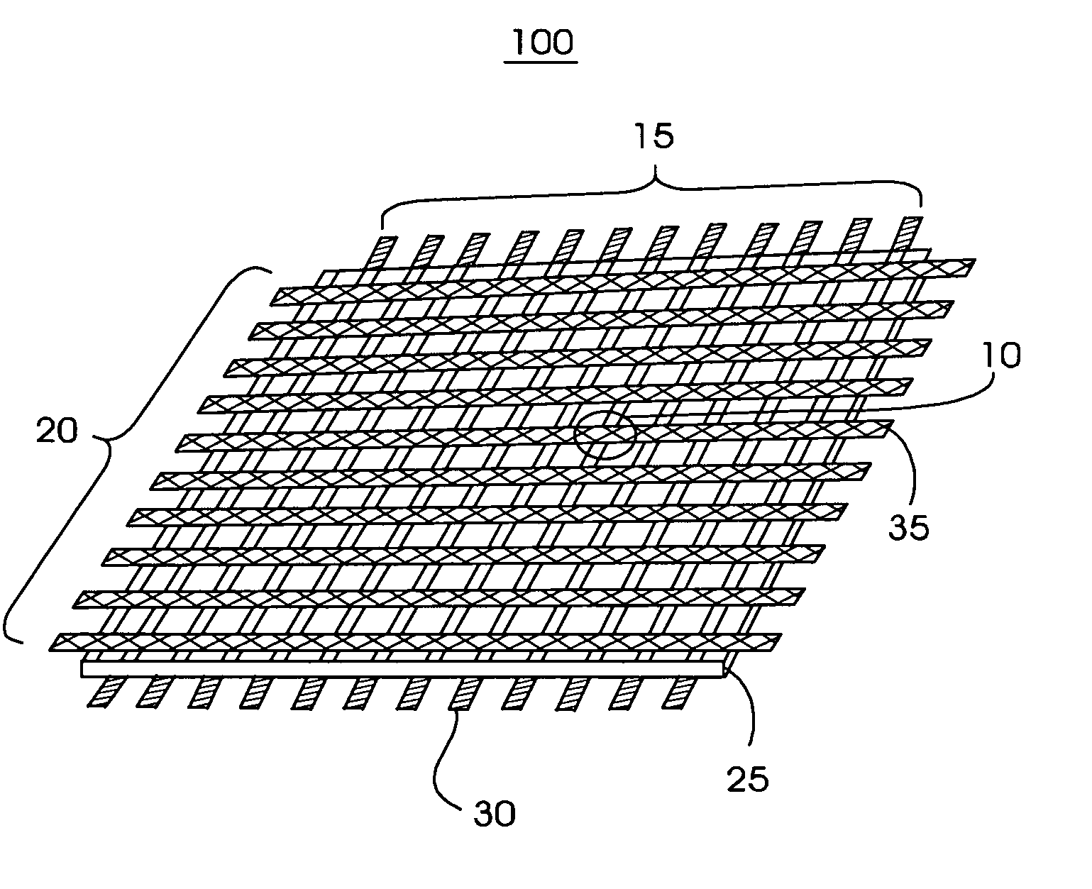
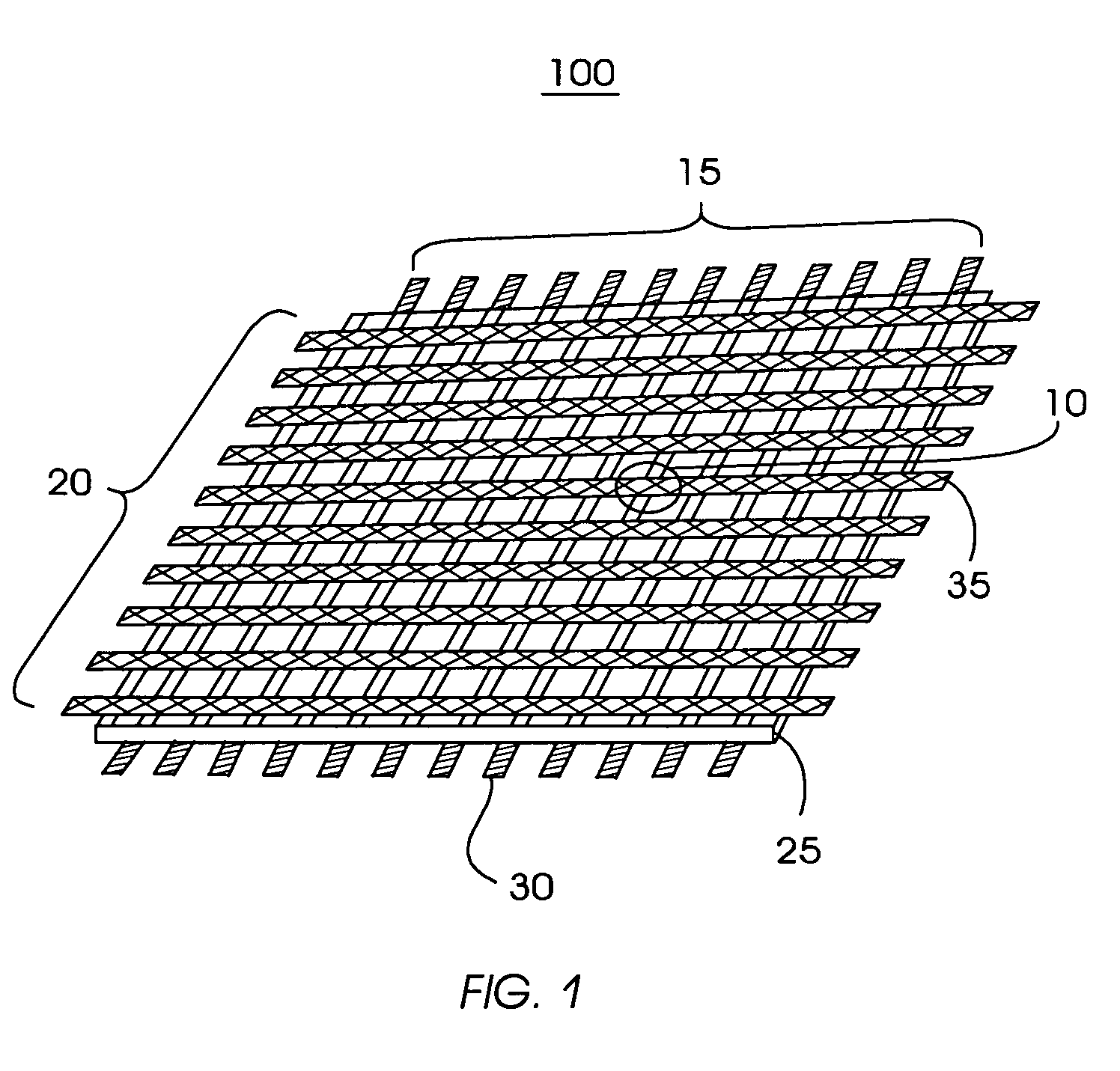
[0039]FIG. 1 illustrates an exemplary high-level architecture of a crosspoint memory array (or system) 100 comprised of a plurality of multi-stable devices 10 may be used. When used as a memory device, the multi-stable device 10 performs at one of two different electrical resistance values, an “on” value or an “off” value, that can be externally set by applying a voltage pulse to the multi-stable device 10. The “on” value may, for example, represent a “1” bit while the “off” value may represents a “0” bit of data. The resistance of the multi-stable device 10 can be read by applying a lower voltage to the multi-stable device 10; the “read” voltage does not affect the state of the multi-stable device 10.

[0040] The crosspoint memory array 100 is formed of an array of electrodes 15 and electrodes 20 that are disposed perpendicularly relative to each other. Electrodes 15 and electrodes 20 may also be disposed at any other relative angular orientations, such that electrodes 15, 20 inters...


PUM


Abstract

A multi-stable memory or data storage element is used in crosspoint data-storage arrays, as a switch, a memory device, or as a logical device. The general structure of the multi-stable element comprises a layered, composite medium that both transports and stores charge disposed between two electrodes. Dispersed within the composite medium are discrete charge storage particles that trap and store charge. The multi-stable element achieves an exemplary bi-stable characteristic, providing a switchable device that has two or more stable states reliably created by the application of a voltage to the device. The voltages applied to achieve the “on” state, the “off” state, any intermediate state, and to read the state of the multi-stable element are all of the same polarity.

Description

PRIORITY CLAIM [0001] The present invention application is a divisional of, and claims the priority of, co-pending U.S. patent application, Ser. No.10 / 645,240, filed on Aug. 20, 2003, titled “Non-Volatile Multi-Stable Memory Device and Methods of Making and Using the Same,” which is incorporated herein by reference. FIELD OF THE INVENTION [0002] The present invention generally relates to memory and storage systems, and particularly to a crosspoint data storage array utilizing a multi-stable device. Specifically, this invention pertains to a multi-stable device comprising a layered, composite medium that utilizes a layer of discrete charge storage particles within the composite medium, to create a device with multiple stable and reproducible values of resistance suitable, for use, for example, as a memory storage device, a switch, or a logical circuit. BACKGROUND OF THE INVENTION [0003] The two conventional common non-volatile data storage devices are: disk drives and solid state ran...

Claims


Application Information

Patent Timeline
Patent Type & Authority Applications(United States)
IPC IPC(8): G11C7/00G11C13/00H01L27/10H01L27/24H01L29/76H01L45/00
CPCB82Y10/00B82Y30/00G11C13/00G11C13/0014G11C13/004G11C13/0069H01L27/2472G11C2213/77H01L27/101H01L45/10H01L45/1233H01L45/14H01L45/1608G11C2013/009H10B63/82H10N70/25H10N70/826H10N70/881H10N70/021
Inventor BOZANO, LUISA DOMINICACARTER, KENNETH RAYMONDSCOTT, JOHN CAMPBELL
Owner GLOBALFOUNDRIES US INC
Why Eureka
Try Eureka