Substrate with a multilayer reflection film, reflection type mask blank for exposure, reflection type mask for exposure and methods of manufacturing them

a multi-layer reflection film and substrate technology, applied in the field of multi-layer reflection film coating substrates, can solve the problems of film peeling, weak adhesion of cron film to glass substrates, and possible dielectric breakdown, so as to prevent particle occurrence and minimize surface defects

Inactive Publication Date: 2005-10-27
HOYA CORP
View PDF12 Cites 45 Cited by
  • Summary
  • Abstract
  • Description
  • Claims
  • Application Information

AI Technical Summary

Benefits of technology

[0062] According to the structure 12, the reflection type mask blank for exposure obtained by the structure 11 is used, and the pattern is formed on the absorber film to produce the reflection type mask for exposure. Thus, it is possible to obtain the reflection type mask for exposure free from pattern defects caused by the particles.
[0063] According to this invention, it is possible to prevent occurrence of particles due to the film peeling of the conductive film upon electrostatic chucking of the substrate provided with the conductive film or the abnormal discharge. As a result, by forming the multilayer reflection film for reflecting the exposure light on the substrate held by the electrostatic chuck, it is possible to obtain the multilayer-reflection-f

Problems solved by technology

Therefore, dielectric breakdown may be caused to occur.
This results in the following problems.
First, adhesion of the CrON film to the glass substrate is weak.
Under this circumstance, warping of the substrate or the like upon electrostatic chucking easily leads to film peeling.
Therefore, depending upon film deposition conditions, abnormal discharge may occur during deposition of the multilayer reflection film or the absorber film.
Upon occurrence of particles due to the film peeling of the conductive film during the electrostatic chucking (during deposition) or the abnormal discharge during deposition, a product (t

Method used


Image

  • Substrate with a multilayer reflection film, reflection type mask blank for exposure, reflection type mask for exposure and methods of manufacturing them
  • Substrate with a multilayer reflection film, reflection type mask blank for exposure, reflection type mask for exposure and methods of manufacturing them
  • Substrate with a multilayer reflection film, reflection type mask blank for exposure, reflection type mask for exposure and methods of manufacturing them

Examples


example 1

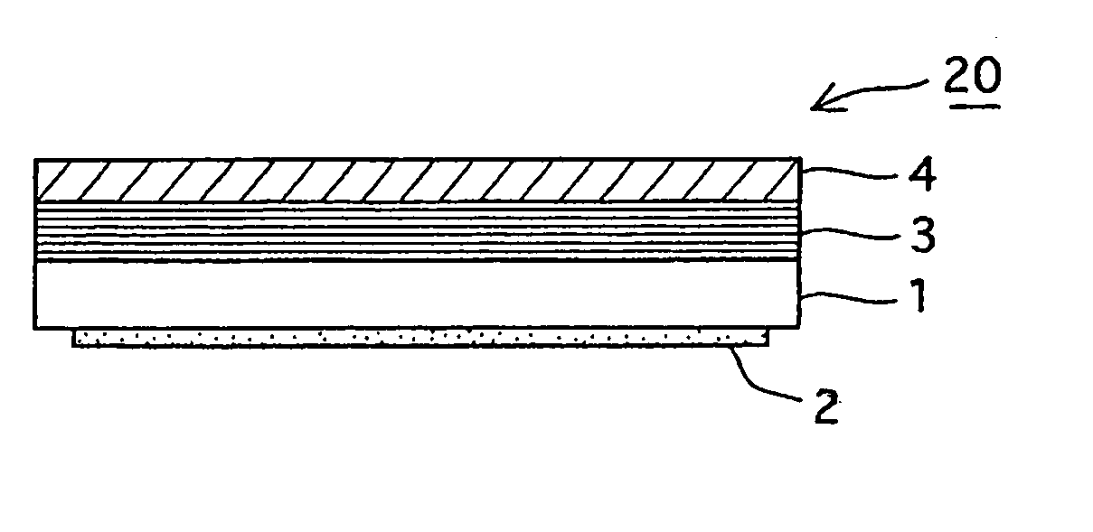
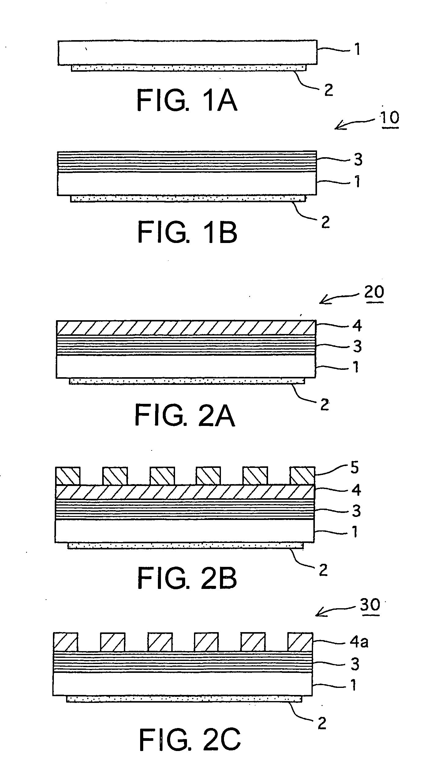
[0113] As the substrate, an SiO2—TiO2 based glass substrate having an outer dimension of 6 inch square and a thickness of 6.3 mm was prepared. The glass substrate had a smooth surface of 0.12 nm Rms and a flatness of 100 nm or less by mechanical polishing.

[0114] Then, the glass substrate was placed at a predetermined position of the holder 60 having the structure shown in FIG. 5 through FIG. 7, and sputter deposition of the conductive film was performed by the use of an inline type sputtering apparatus. At first, by using a chromium target, reactive sputtering was carried out in a mixed gas atmosphere of argon (Ar) and nitrogen (N) (Ar: 72 volume %, N2: 28 volume %, pressure: 0.3 Pa) to form a CrN film having a thickness of 15 nm. Successively, by using a chromium target, reactive sputtering was carried out in a mixed gas atmosphere of argon and methane (Ar: 96.5 volume %, CH4: 3.5 volume %, pressure: 0.3 Pa) to form a CrC film having a thickness of 25 nm. Finally, by using a chrom...

example 2

[0123] In this example, the multilayer-reflection-film-coated substrate was produced in the manner similar to the example 1 except that the conductive film formed on the substrate had a double-layer structure of CrCN / CrON films. The deposition method of the CrON film was similar to that in the example 1. The deposition of the CrCN film was carried out by the use of the chromium target and by adjusting gas flow rates of methane and nitrogen in a mixed gas atmosphere of argon, methane, and nitrogen. The film thickness was 60 nm. In the obtained CrCN film, the carbon content was 8 at % and the nitrogen content was 12 at %. In the manner similar to the example 1, the conductive film was formed in an area 10 mm inside from the side surface of the substrate.

[0124] For the multilayer-reflection-film-coated substrate thus obtained in this example, the number of particles on the surface of the multilayer reflection film was measured. As a result, the number was 1.0 defects / cm2. Thus, genera...

example 3

[0127] In this example, the conductive film formed on the substrate was a lamination film having a three-layer structure of CrN / CrC / CrON similar to that of the example 1. The conductive film was formed throughout an entire area of one surface of the substrate, including one principal surface of the substrate as well as the chamfered surface and the side surface of the substrate. In the manner similar to example 1 except the above-mentioned respect, the multilayer-reflection-film-coated substrate was produced. For the multilayer-reflection-film-coated substrate thus obtained in this example, the number of particles on the surface of the multilayer reflection film was measured. As a result, the number was 10 defects / cm2. Thus, the number of the particles generated upon depositing the multilayer reflection film was small. In this example, the conductive film was formed also on the chamfered surface and the side surface of the substrate. However, since the conductive film comprising the...


PUM

PropertyMeasurementUnit
Electrical conductoraaaaaaaaaa
Reflectionaaaaaaaaaa

Abstract

A multilayer-reflection-film-coated substrate includes a substrate, a multilayer reflection film formed on the substrate and reflecting an exposure light, and a conductive film formed on an opposite side of the substrate from the multilayer reflection film in a region excluding at least a peripheral portion of the substrate. The conductive film is made of a material containing chromium (Cr). The conductive film contains nitrogen (N) on a substrate side and at least one of oxygen (O) and carbon (C) on a surface side. A reflection type mask blank for exposure is obtained by forming an absorber film for absorbing the exposure light on the multilayer reflection film of the multilayer-reflection-film-coated substrate. A reflection type mask is obtained by forming a pattern on the absorber film of the reflection type mask blank for exposure.

Description

[0001] This application claims priority to prior Japanese patent application JP2003-429072, the disclosure of which is incorporated herein by reference. BACKGROUND OF THE INVENTION [0002] This invention relates to a multilayer-reflection-film-coated substrate having a multilayer reflection film formed on a substrate and reflecting exposure light, a reflection type mask blank for exposure using the above-mentioned substrate, and a reflection type mask for exposure as well as methods of manufacturing them. [0003] Recently, in the semiconductor industry, the EUV lithography (EUVL), which is an exposure technique using extreme ultra violet (Extreme Ultra Violet, EUV) light, is promising following miniaturization of a semiconductor device. It is noted here that the EUV light means light of a wavelength band within a soft X-ray region or a vacuum ultraviolet region, specifically, light having a wavelength of about 0.2-100 nm. As a mask used in the EUV lithography, proposal is made of a re...

Claims


Application Information

Patent Timeline
IPC IPC(8): B32B17/06C03C17/34C03C17/36G03F1/22G03F1/24G03F1/40H01L21/027
CPCB82Y10/00G21K2201/067C03C17/3435C03C17/3441C03C17/36C03C17/3618C03C17/3626C03C17/3649C03C17/3665C03C2218/328C03C2218/33G03F1/14G03F1/24G03F1/38G03F7/707G03F7/70708B82Y40/00
Inventor KINOSHITA, TAKERUHOSOYA, MORIOSHOKI, TSUTOMU
Owner HOYA CORP
Why Eureka
Try Eureka