Plasma etching method

a technology of plasma etching and plasma, which is applied in the direction of beds, beds, seating furniture, etc., can solve the problems of occurrence of residues, anomalous etch suspension, and serious troubles, and achieve stable plasma etching, stable continuous plasma etching, and prevent the deposition of residues

Inactive Publication Date: 2005-11-10
SONY CORP
View PDF4 Cites 37 Cited by
  • Summary
  • Abstract
  • Description
  • Claims
  • Application Information

AI Technical Summary

Benefits of technology

[0008] It is desirable to provide a method for plasma etching an insulating layer by using a plasma etching equipment and a fluorocarbon etching gas, the method being able to perform stable plasma etching without causing deposition on the plasma surround parts.
[0009] The above-mentioned desire is achieved by the first embodiment of the present invention which is concerned with a method for plasma etching an insulating layer by using a plasma etching equipment and a fluorocarbon etching gas, the method including controlling the sheath potential (Vs) that appears on the outermost surface of the plasma surrounding parts of the plasma etching equipment in response to the value of F0 / C0, where C0 and F0 each denote the total amount of carbon atoms and fluorine atoms constituting the fluorocarbon etching gas, so as to avoid deposition on the plasma surrounding parts.
[0011] The above-mentioned desire is achieved by the second embodiment of the present invention which is concerned with a method for plasma etching each layer of an object of M-layered structure (M≧2) having at least one insulating layer by using a plasma etching equipment and a fluorocarbon etching gas, the method including controlling the sheath potential Vm-s that appears on the outermost surface of the plasma surrounding parts of the plasma etching equipment when the mth layer (m=1, 2, . . . M) undergoes plasma etching, in response to the value of Fm-0 / Cm-0, where Cm-0 and Fm-0 each denote the total amount of carbon atoms and fluorine atoms constituting the fluorocarbon etching gas used for plasma etching of the mth layer, so as to avoid deposition on the plasma surrounding parts.
[0013] The plasma etching method according to the first and second embodiments of the present invention controls the sheath potential Vs or Vm-s which occurs on the outermost surface of the plasma surrounding parts during plasma etching. The sheath potential is the ion accelerating voltage and it is also an electric field applied onto the sheath that appears in contact with the surface of the plasma surrounding parts. The sheath is a thin layer of ions spontaneously accumulating on the surface of the plasma surrounding parts, and it prevents the inflow of excess electrons. The magnitude of the electric field equals the difference between the potential of plasma and the potential of the plasma surrounding parts.
[0030] The plasma etching method according to an embodiment of the present invention includes a step of controlling the sheath potential Vs or Vm-s that appears on the outermost surface of the plasma surrounding parts, in response the value of F0 / C0 or Fm-0 / Cm-0 of the fluorocarbon gas. In this way it is possible to certainly prevent deposition of residues on the plasma surrounding parts. The absence of deposition on the plasma surrounding parts permits stable plasma etching even when the object for etching and the etching gas are changed. It also permits stable plasma etching on insulating layers formed from a low dielectric constant material which is vulnerable to plasma fluctuation. Another advantage is that the plasma surrounding parts remain unchanged at the start of and during plasma etching on an object of laminate structure. This leads to stable continuous plasma etching. Thus the plasma etching method of the present invention meets requirements for accurate fabrication necessary for miniaturization and is applicable to any object of complex laminate structure without causing serious troubles such as line width fluctuation, anomalous etching suspension, and residue occurrence.
[0031] As mentioned above, the present invention permits accurate plasma etching on fine laminate layers sensible to fluctuation. In addition, it permits continuous plasma etching in a single plasma etching equipment. This permits the production facility to run with a less number of equipments in high yields, which leads to cost saving in plasma etching process.

Problems solved by technology

The consequence of narrow latitude is that even the slightest deviation from the predetermined plasma etching condition causes serious troubles such as anomalous line width, anomalous etch suspension, and occurrence of residues.
Unfortunately, there is an instance where residues deposit on the plasma surrounding parts during plasma etching as schematically indicated by solid lines in FIG. 6.
This causes fluctuations in plasma etching conditions.

Method used


Image

  • Plasma etching method
  • Plasma etching method
  • Plasma etching method

Examples


example 1

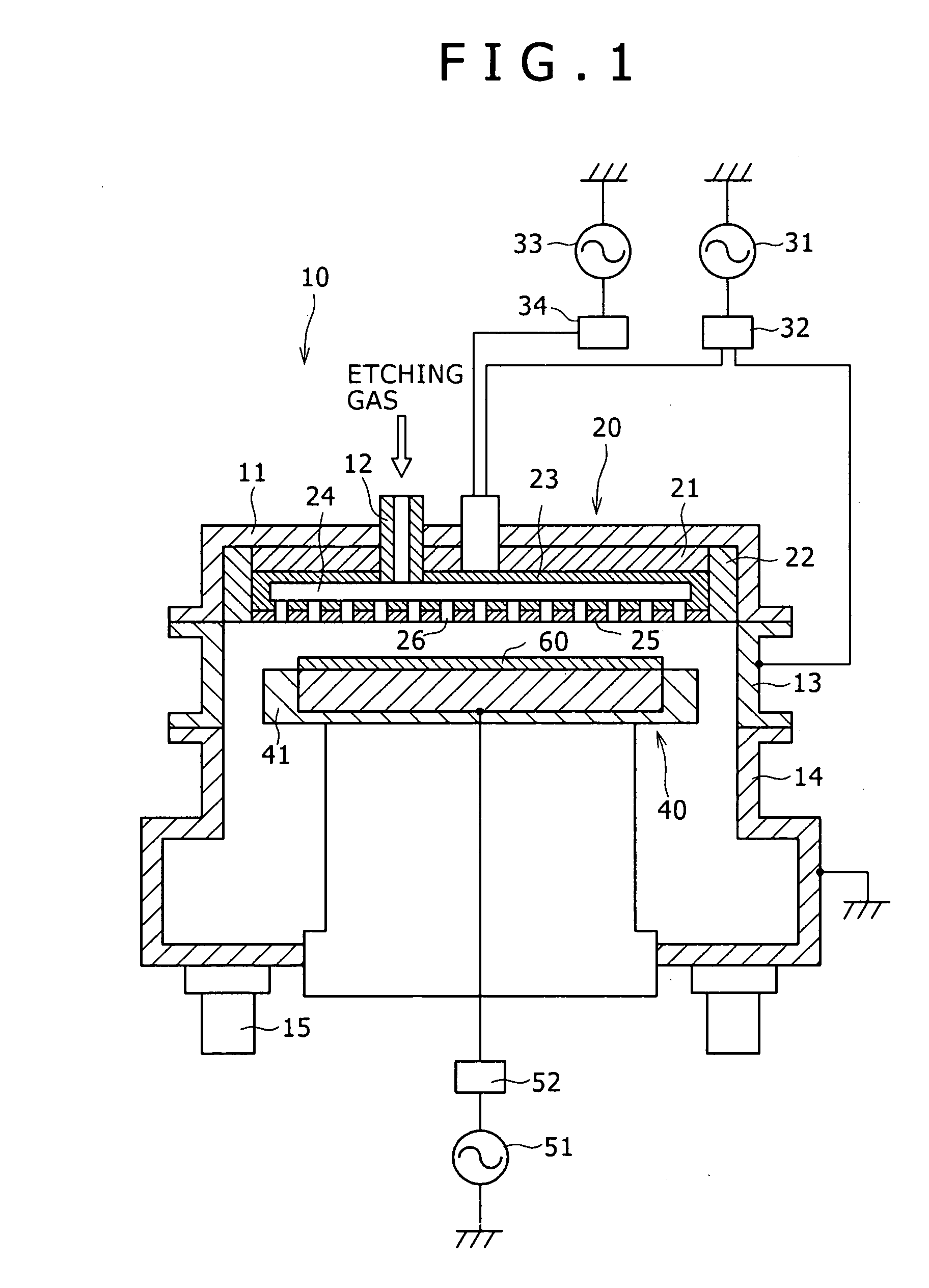
[0039] This example demonstrates the plasma etching method according to a first embodiment of the present invention. Plasma etching in this example employs the parallel flat plate type plasma etching equipment as shown in FIG. 1 which is referred to as etching equipment 10 hereinafter. The etching equipment 10 has the upper electrode 20 arranged in its upper part and also has the lower electrode 40 arranged in its lower part. The upper and lower electrodes 20 and 40 are parallel and opposed to each other. The upper and lower electrodes 20 and 40 are supplied with high frequency power, so that an electric field is induced between them. This electric field generates a plasma which dissociates or ionizes the etching gas introduced into the etching equipment 10. The resulting particles move to the surface of the substrate, at which they bring about reaction for plasma etching on the insulating layer etc.

[0040] The upper electrode 20 includes the circular-plate-like conducting member 21...

example 2

[0059] This example demonstrates the plasma etching method according to a second embodiment of the present invention. Plasma etching in this example was performed by using the etching equipment 10 schematically shown in FIG. 1.

[0060] In Example 2, plasma etching was performed on two insulating layers, with the upper layer (the first layer) formed from SiO2 and the lower layer (the second layer) formed from SiOCH. The two insulating layers are regarded as the M-layered object for plasma etching (M=2 in this case). The etching gas is a fluorocarbon gas.

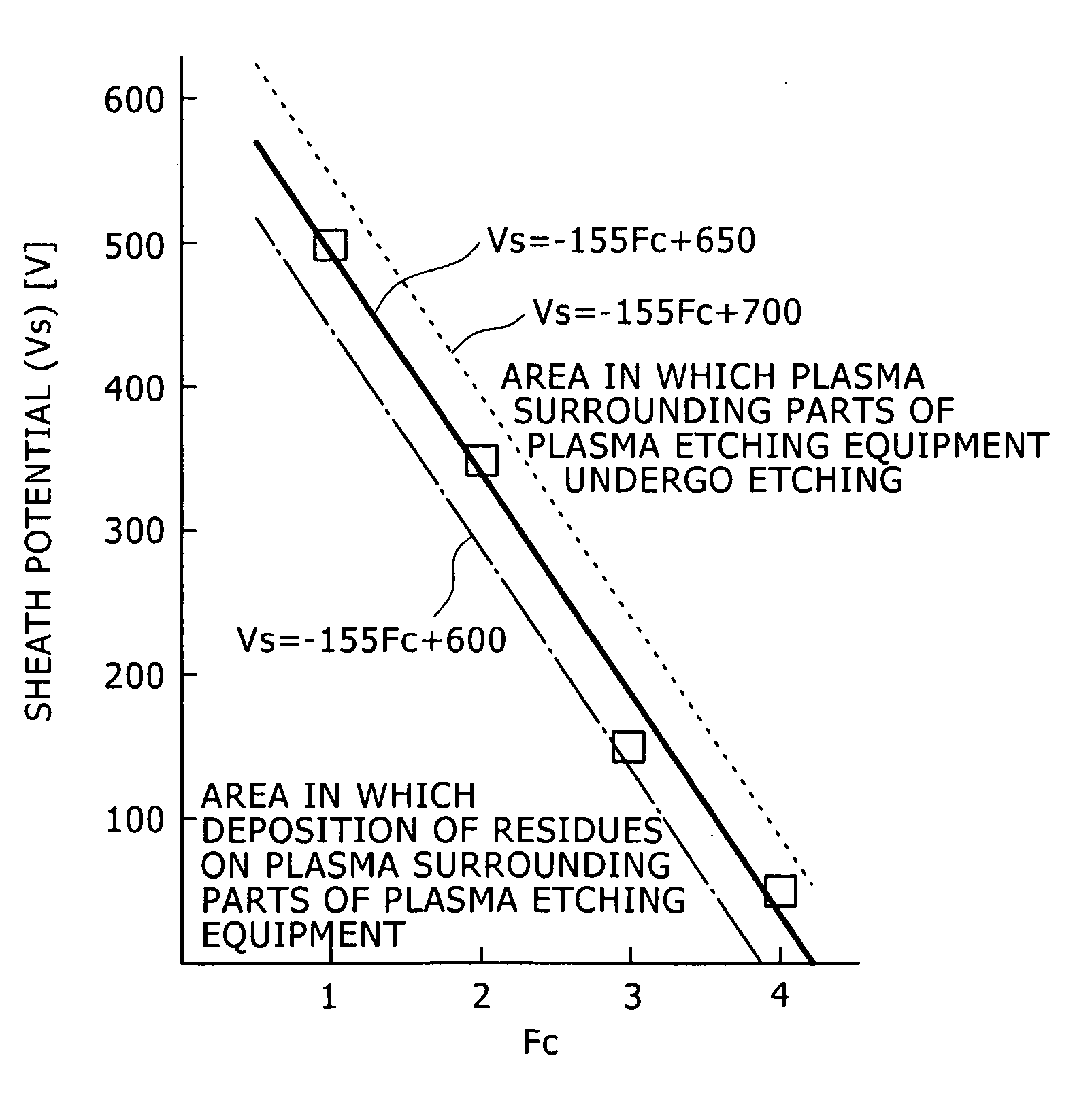
[0061] When plasma etching is performed on the mth layer, the sheath potential Vm-s, which appears on the outermost surface of the plasma surrounding parts, is controlled in response to the value of Fm-0 / Cm-0, where Cm-0 and Fm-0 denote respectively the number of carbon atoms and the number of fluorine atoms in the fluorocarbon gas used for plasma etching on the mth layer (m=1, 2, . . . M), so that no deposition of residues occurs on ...

example 3

[0068] This example is a modification of Example 2. In Example 3, plasma etching was performed on an object of three-layered structure to make openings for via holes. The upper layer (the first layer) is a masking layer formed from SiO2. The intermediate layer (the second layer) is an insulating layer formed from SiOCH. The lower layer (the third layer) is an etch stop layer formed from SiCN. The three-layered object for plasma etching substantially has M=2. There is a patterned resist layer on the mask layer formed from SiO2.

[0069] To be concrete, plasma etching was performed on the mask layer (the first layer) of SiO2 and the insulating layer (the second layer) of SiOCH under the conditions shown in Table 6 below. Plasma etching on the first and second layers was performed with the same fluorocarbon gas under the same conditions. In other words, both the sheath potential V1-s and the sheath potential V2-s were kept at the same value because the values of F1-0 / C1-0 and F2-0 / C2-0 a...


PUM

PropertyMeasurementUnit
thicknessaaaaaaaaaa
relative permittivityaaaaaaaaaa
thicknessaaaaaaaaaa

Abstract

A method for plasma etching an insulating layer by using a fluorocarbon etching gas, the method including controlling the sheath potential Vs (or ion accelerating voltage) that appears on the outermost surface of the plasma surrounding parts of the plasma etching equipment in response to the value (Fc) of F0 / C0, where C0 and F0 each denote the total amount of carbon atoms and fluorine atoms constituting the fluorocarbon etching gas, so as to avoid deposition of residues on the plasma surrounding parts. This method permits stable plasma etching.

Description

BACKGROUND OF THE INVENTION [0001] The present invention relates to a plasma etching method. [0002] The recent development of ULSI devices aims at fast operation and low power consumption. For this purpose, the latest ULSI devices usually have insulating layers formed from a low dielectric constant material and multi-level interconnections formed from copper. In this connection, there is an increasing demand for continuously performing plasma etching on an object of laminate structure in the same plasma etching equipment. Plasma etching is becoming more complex than before as the result of recent technical advance including adoption of low dielectric constant materials (which are vulnerable to variation in plasma etching), more stringent requirements for fabrication precision accompanied by miniaturization, and diversified objects of laminate structure to be etched. [0003] Complexity of plasma etching will be understood from FIG. 5 which illustrates how the etch rate varies in plasm...

Claims


Application Information

Patent Timeline
Patent Type & Authority Applications(United States)
IPC IPC(8): C23F1/00H01L21/302H01L21/3065H01L21/311
CPCH01L21/31116A47C19/022A47C21/00
Inventor TATSUMI, TETSUYA
Owner SONY CORP
Why Eureka
Try Eureka