Method of fabricating liquid crystal display device

a liquid crystal display and liquid crystal technology, applied in the direction of semiconductor devices, radio frequency controlled devices, instruments, etc., can solve the problems of inability to completely suppress such etching residues, method unavoidably carries out annealing steps twice, and inability to design the method to include only one annealing step, etc., to prevent contact resistance and poor display quality

Inactive Publication Date: 2005-11-10
NEC LCD TECH CORP
View PDF7 Cites 8 Cited by
  • Summary
  • Abstract
  • Description
  • Claims
  • Application Information

AI Technical Summary

Benefits of technology

[0029] In view of the above-mentioned problems in the conventional methods, it is an object of the present invention to provide a method of fabricating a liquid crystal display device which method is capable of forming a contact hole throughout an electrically insulating organic or inorganic interlayer film and accurately patterning an electrically conductive transparent film into a pixel electrode uniformly within a substrate without etching residue of the electrically conductive transparent film, and further of preventing a contact resistance between the electrically conductive transparent film and an underlying metal film from increasing, ensuring no poor quality in displayed images.
[0049] In accordance with the present invention, an amorphous indium-tin oxide film is formed on an interlayer insulating film in a predetermined pattern, and then, the amorphous indium-tin oxide film is poly-crystallized by thermal annealing carried out after formation of an alignment film. Thus, the present invention makes it possible to pattern an indium-tin oxide film to a pixel electrode with accuracy and uniformity, but without etching residue. In particular, the present invention makes it possible, in an in-plane switching type liquid crystal display device including a common electrode and a pixel electrode both comprised of an indium-tin oxide film on an interlayer insulating film, to prevent non-uniformity in displayed images, caused by non-uniformity in patterning the indium-tin oxide film, and further to enhance a fabrication yield.
[0050] In addition, the present invention makes it possible to reduce an annealing step by one.
[0051] The present invention makes it possible, in a liquid crystal display device including an interlayer insulating film comprised of an electrically insulating organic film and an electrically insulating inorganic film and formed on a thin film transistor, to accurately and uniformly pattern an electrically conductive transparent film, and prevent a contact resistance between the electrically conductive transparent film and an underlying metal film, by applying helium (He) plasma to an interlayer insulating film prior to formation of a contact hole throughout the electrically insulating inorganic film. In particular, the present invention makes it possible, in an in-plane switching type liquid crystal display device including a common electrode and a pixel electrode both comprised of an electrically conductive transparent film on an interlayer insulating film, to prevent non-uniformity in displayed images, caused by non-uniformity in patterning the electrically conductive transparent film or by an increased contact resistance, and further to enhance a fabrication yield.

Problems solved by technology

Accordingly, it is impossible to design the method to include only one annealing step.
If indium-tin oxide is deposited at 100 degrees centigrade or lower, such etching residue can be suppressed to some degree, but it is not possible to completely suppress such etching residue.
Since the method includes a step of carrying out annealing after deposition of indium-tin oxide, the method unavoidably carries out an annealing step twice.
By carrying out sputter etching or dry etching in a condition in which the electrically insulating organic film has been already formed, an etching apparatus might be contaminated with the result of significant reduction in productivity, and a roughened surface of the electrically insulating organic film would be planarized during baking the electrically insulating organic film.
If sputter etching or dry etching is carried out after formation of a contact hole, there is caused a problem that the above-mentioned contact resistance is increased.
Increase in a contact resistance might cause horizontal cross-talk and / or non-uniformity of horizontal lines in a common-storage type twisted nematic liquid crystal display device or an in-plane switching type liquid crystal display device.
However, if a thin film transistor is designed to have a structure in which common lines are bound to one another through an indium-tin oxide film formed on an interlayer insulating film, a contact resistance would be increased due to an electrically insulating organic film, and hence, the common lines would unavoidably have a high resistance.
If process control for a step of patterning an electrically conductive transparent film into a pixel electrode is insufficient, there would be resulted in non-uniformity in displayed images.

Method used


Image

  • Method of fabricating liquid crystal display device
  • Method of fabricating liquid crystal display device
  • Method of fabricating liquid crystal display device

Examples


first embodiment

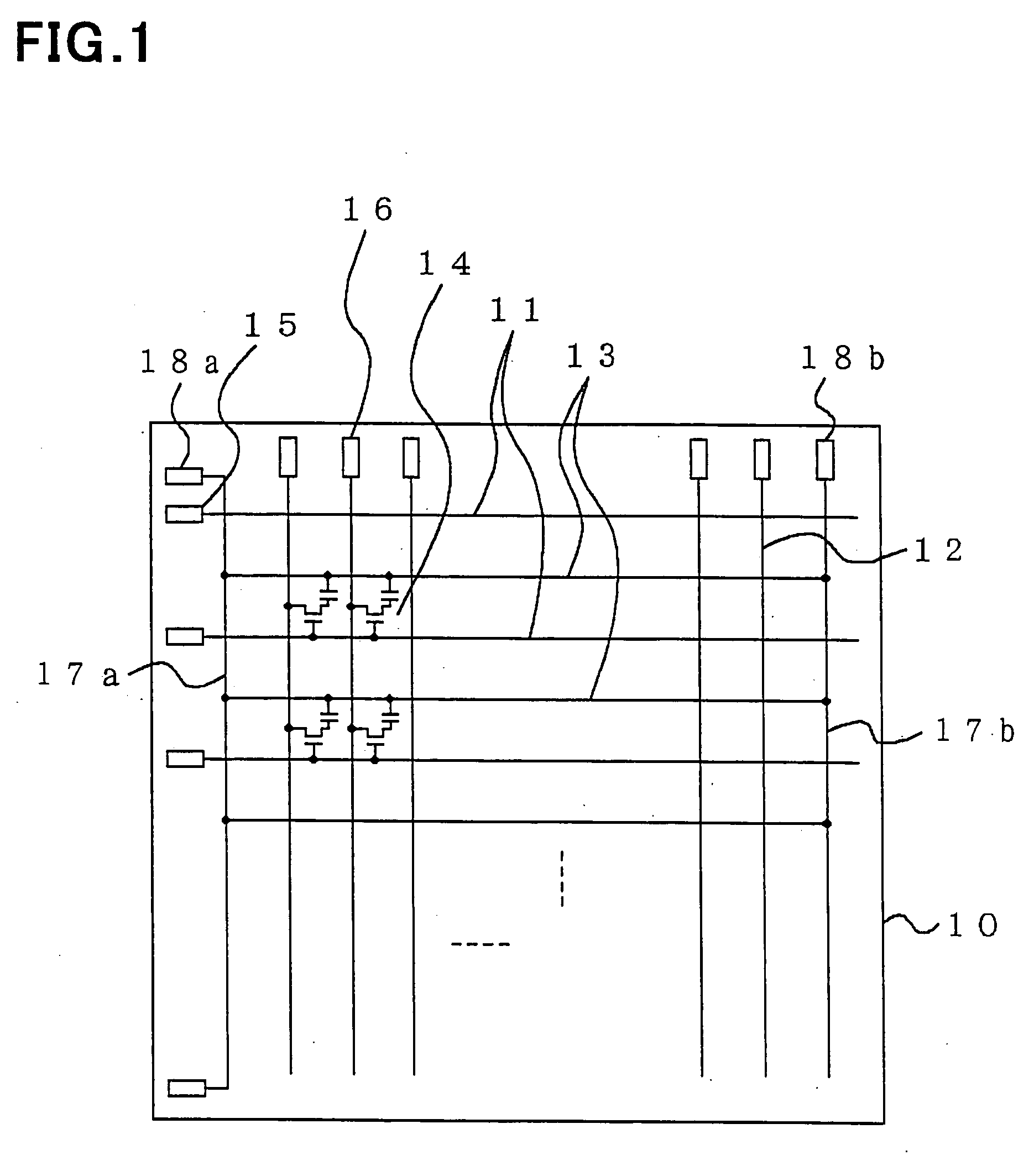
[0083]FIG. 1 is a plan view of a substrate on which a thin film transistor (TFT) is to be fabricated, in a liquid crystal display device fabricated by a method in accordance with the first embodiment of the present invention. In the first embodiment, an in-plane switching type liquid crystal display device is fabricated. Hereinbelow, the substrate is referred to simply as a TFT substrate.

[0084] As illustrated in FIG. 1, the TFT substrate 10 includes, on a surface thereof facing an opposing substrate, a plurality of scanning lines 11, a plurality of signal lines 12 each extending perpendicularly to the scanning lines 11, and a plurality of common lines 13 each extending between adjacent scanning lines 11 in parallel with the scanning lines 11. Thin film transistors (TFTs) 14 are fabricated in a matrix at intersections of the scanning lines 11 with the signal lines 12.

[0085] Each of the scanning lines 11 is connected at an end thereof to a scanning line terminal 15. A drive signal i...

second embodiment

[0140] In the second embodiment, plasma is applied onto the electrically insulating organic film 33.

[0141] The steps in the first embodiment, having been explained with reference to FIGS. 2 to 11C are carried out. Thus, the electrically insulating organic film 33 is now formed on the passivation film 32.

[0142] Then, helium (He) plasma is applied all over to a resultant. Application of helium plasma is carried out by discharging helium gas at high frequency in a dry-etching apparatus, for instance.

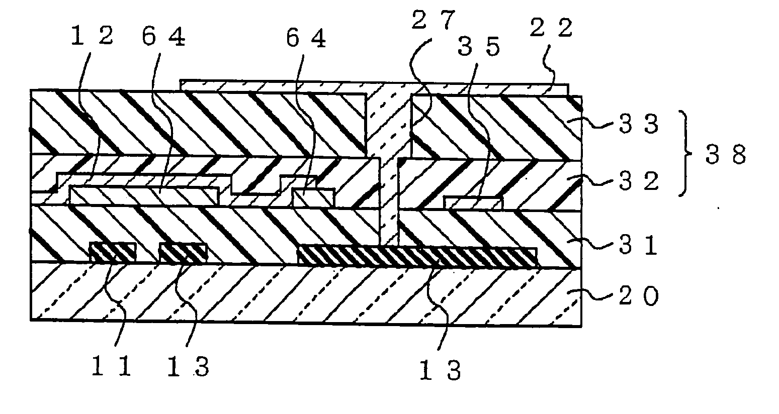
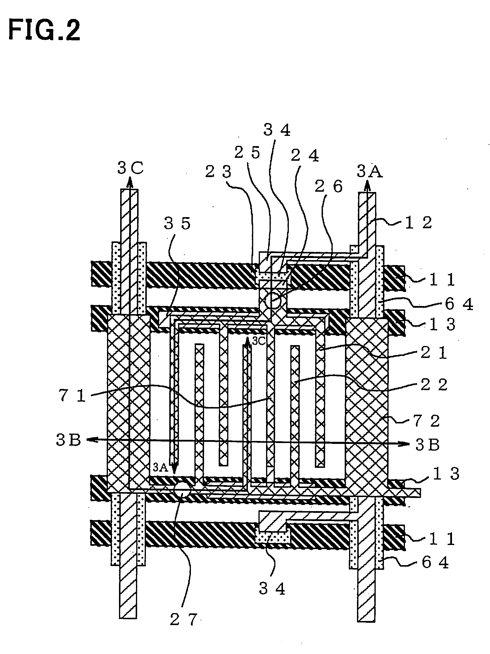
[0143] Thereafter, as illustrated in FIGS. 12 and 13A to 13C, the passivation film 32 is etched by photolithography to thereby form the contact hole 26 (see FIG. 13A) in alignment with the hole 66, through which the source electrode 24 is exposed, and a contact hole (not illustrated) through which a metal film of the signal-line terminal 16 is exposed. Concurrently, the passivation film 32 and the gate insulating film 31 are etched to form the contact hole 27 (see FIG. 13C) in alignment ...


PUM

PropertyMeasurementUnit
temperatureaaaaaaaaaa
crystal diameteraaaaaaaaaa

Abstract

The method of fabricating a liquid crystal display device includes the steps of (a) fabricating a switching device on a substrate, (b) forming an interlayer insulating film on the substrate such that the switching device is covered with the interlayer insulating film, and (c) forming a transparent electrode on the interlayer insulating film, the transparent electrode being electrically connected to the switching device through the interlayer insulating film, the step (c) including (c1) depositing electrically conductive, transparent and amorphous material on the interlayer insulating film, (c2) patterning the material into the transparent electrode, and (c3) turning the transparent electrode into polysilicon by thermal annealing carried out after formation of an alignment film.

Description

CROSS REFERENCE TO RELATED APPLICATIONS [0001] This application is a division of co-pending application Ser. No. 10 / 692,736, filed on Oct. 27, 2003, the entire contents of which are hereby incorporated by reference.BACKGROUND OF THE INVENTION [0002] 1. Field of the Invention [0003] The invention relates to a method of fabricating a liquid crystal display device, and more particularly to such a method including the step of forming an electrically conductive transparent film in a predetermined pattern on an interlayer insulating film comprised of an electrically insulating organic film. [0004] 2. Description of the Related Art [0005] A liquid crystal display device is grouped into a light-transmission type one, a light-reflection type one and a combination type one in dependence on a light source. [0006] A light-transmission type liquid crystal display device is designed to include a back-light device as a light source for displaying images. A light-reflection type liquid crystal disp...

Claims


Application Information

Patent Timeline
Patent Type & Authority Applications(United States)
IPC IPC(8): G02F1/1343G02F1/1362G02F1/1333G02F1/1368H01L21/77H01L21/84H01L27/146H01L29/15
CPCG02F1/134363G02F1/136227H01L27/1248H01L27/14621H01L27/124G02F2202/104
Inventor HAYASE, TAKASUKEYAMADA, KEIKOYAMASHITA, MASAMINAKATA, SHINICHIMAEDA, AKITOSHI
Owner NEC LCD TECH CORP
Why Eureka
Try Eureka