Semiconductor display device and driving method

a display device and semiconductor technology, applied in the direction of instruments, computing, electric digital data processing, etc., can solve the problems of reducing image quality, affecting the stability of the device, and affecting the effect of the display device, so as to promote the lattice distortion, improve stability, and shorten the range order

Inactive Publication Date: 2005-11-24
SEMICON ENERGY LAB CO LTD
View PDF4 Cites 19 Cited by
  • Summary
  • Abstract
  • Description
  • Claims
  • Application Information

AI Technical Summary

Benefits of technology

[0023] A semi-amorphous semiconductor has an intermediate structure between amorphous and crystalline (including single crystalline and polycrystalline) structures. The semi-amorphous semiconductor has a third state that is stable in terms of free energy, and has a short range order and a lattice distortion, in which crystals having a particle size of 0.5 to 20 nm can be dispersed in a non-single crystalline semiconductor. In the semi-amorphous semiconductor, Raman spectrum is shifted to the lower frequency band than 520 cm−1 and diffraction peaks of (111) and (220) believed to be derived from a Si crystal lattice are observed by X-ray diffraction. Further, the semiconductor is mixed with hydrogen or halogen of at least 1 atom % for terminating the dangling bond. Such a semiconductor is called herein a semi-amorphous semiconductor (SAS) for convenience. A favorable semi-amorphous semiconductor with improved stability can be obtained by further promoting the lattice distortion by mixing rare-gas elements such as helium, argon, krypton, and neon.
[0024] According to the above-described structure of the invention, the total gray scale level and the number of subframe periods are not required to be equal to each other unlike a conventional structure, display can be performed with a high total gray scale level while suppressing the number of subframes. Consequently, the total gray scale level can be increased without performing processing such as dithering that decreases image quality.
[0025] In addition, driving is performed so as to fulfill a sharing ratio higher than a required value, so that a pseudo contour can be prevented while suppressing the frame frequency and the drive frequency of a driver circuit.

Problems solved by technology

However, in the case of performing display using the time gray scale method, there is a problem in that a pseudo contour may be displayed in a pixel portion depending on the frame frequency.
However, lengthening the frame period is not preferable in that drastic increase of the total gray scale level is not to be realized whereas a pseudo contour is to be more generated.
However, by performing the image processing such as dithering, a large total gray scale level can be displayed while the image is displayed as if sand is spread thereover, leading inevitably to decrease in image quality.

Method used


Image

  • Semiconductor display device and driving method
  • Semiconductor display device and driving method
  • Semiconductor display device and driving method

Examples


embodiment 1

[0086] Next, a circuit diagram of a pixel in a light emitting device of the invention is described using FIGS. 6A to 6C.

[0087]FIG. 6A is an example of an equivalent circuit diagram of a pixel, which comprises a signal line 6114, a power supply line 6115, a scan line 6116, a light emitting element 6113, TFT's 6110 and 6111, and a capacitor 6112. The signal line 6114 is inputted with a video signal by a signal line driver circuit. The TFT 6110 can control supply of potential of the video signal to a gate of the TFT 6111 in accordance with a selection signal inputted into the scan line 6116. The TFT 6111 can control supply of current to the light emitting element 6113 in accordance with the potential of the video signal. The capacitor 6112 can hold gate-source voltage of the TFT 6111. It is to be noted that the capacitor 6112 is provided in FIG. 6A, however, it may be not provided if the gate capacitance of the TFT 6111 or the other parasitic capacitance are enough to hold the gate-so...

embodiment 2

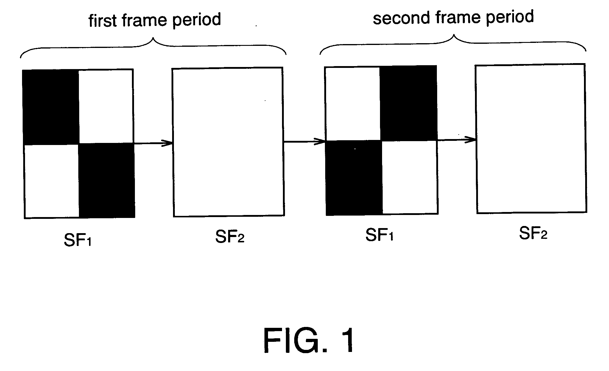
[0091] In this embodiment, timing of appearing each subframe period is described in the case of the driving method described in FIG. 4.

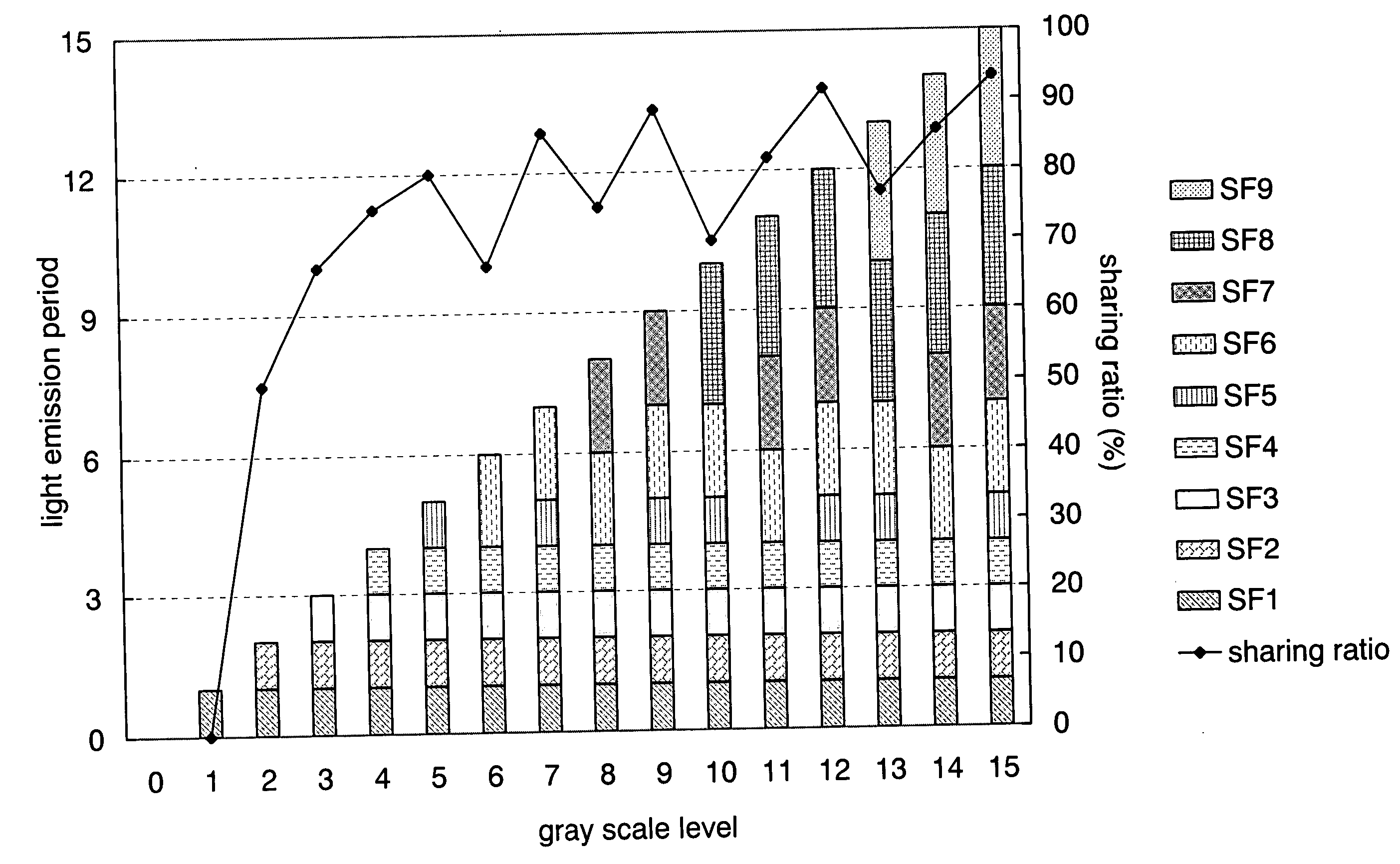
[0092]FIG. 7 is a timing chart for the case of a 4-bit gray scale display using the driving method shown in FIG. 4. In FIG. 7, the horizontal axis indicates the length of subframe periods SF1 to SF9 within one frame period, and the vertical axis indicates the selection sequence of scan lines. The length ratio of the subframe periods SF1 to SF9 is set to be 1:1:1:1:1:2:2:3:3 sequentially from SF1.

[0093] When each subframe period starts, video signal input is performed per pixels for one row sharing the scan line. After the video signal is inputted into the pixel, a light emitting element emits light or no light in accordance with data of the video signal. The light emitting element in each pixel keeps the light emission or non-light emission in accordance with data of the video signal until the next subframe period starts.

[0094] It is to be noted t...

embodiment 3

[0096] In this embodiment, a cross-sectional structure of a pixel where a transistor for controlling current supply to a light emitting element is a P-channel type is described using FIGS. 8A to 8C. Note that, in this specification, one of the anode and the cathode of the light emitting element, of which potential can be controlled by a transistor, is referred to as a first electrode, and the other is referred to as a second electrode. Description is made on the case where the first electrode is the anode and the second electrode is the cathode in FIGS. 8A to 8C, however, it is possible that the first electrode is the cathode while the second electrode is the anode as well.

[0097]FIG. 8A is a cross-sectional view of a pixel where a transistor 6001 is a P-channel type and light from a light emitting element 6003 is extracted from a first electrode 6004 side. The first electrode 6004 of the light emitting element 6003 is electrically connected to the transistor 6001 in FIG. 8A.

[0098]...


PUM


Abstract

The invention provides a semiconductor display device with less generation of a pseudo contour while the drive frequency of a driver circuit is suppressed. Furthermore, the invention provides a semiconductor display device with less generation of a pseudo contour while the decrease in image quality is suppressed. A semiconductor display device comprises a table storing data for determining a relationship between the gray scale level of a video signal and a subframe period for light emission in the plurality of subframe periods, a controller for changing a video signal in accordance with the data and outputting, and a panel whose pixel gray scale level is controlled in accordance with the outputted video signal. The number and the length of the plural subframe periods for each gray scale level of 2 or more are determined in accordance with a subframe ratio RSF which is calculated in accordance with a sharing ratio Rsh determined by the frame frequency.

Description

BACKGROUND OF THE INVENTION [0001] 1. Field of the Invention [0002] The present invention relates to a semiconductor display device for displaying by a time gray scale method and a driving method thereof. [0003] 2. Description of the Related Art [0004] As a driving method of a light emitting device that is one of semiconductor display devices, there is known a time gray scale method in which a light emission period of a pixel in one frame period is controlled with binary voltage of a digital video signal to display a gray scale. Electroluminescent materials are more suitable for a time gray scale method than liquid crystals and the like since the response speed is generally faster. Specifically, when performing display by the time gray scale method, one frame period is divided into a plurality of subframe periods. Then, a pixel emits light or does not emit light according to a video signal in each subframe period. According to the aforementioned structure, the total actual light emi...

Claims


Application Information

Patent Timeline
Patent Type & Authority Applications(United States)
IPC IPC(8): G09G3/20G09G3/22G09G3/32G09G5/00
CPCG09G3/2029G09G3/2033G09G3/22G09G2320/0266G09G2300/0842G09G2320/0261G09G3/3233
Inventor MIYAGAWA, KEISUKE
Owner SEMICON ENERGY LAB CO LTD
Why Eureka
Try Eureka