Low-carbon-doped silicon oxide film and damascene structure using same

a technology of damascene and silicon oxide, which is applied in the direction of semiconductor devices, semiconductor/solid-state device details, electrical apparatus, etc., can solve the problems of stress corrosion crack at the interface, increase the possibility of corrosion at the interface, and reduce the electrical circuit lifetime. , to achieve the effect of enhancing moisture intake, reducing the electrical circuit lifetime, and increasing the possibility of corrosion

Active Publication Date: 2005-11-24
ASM JAPAN
View PDF4 Cites 367 Cited by
  • Summary
  • Abstract
  • Description
  • Claims
  • Application Information

AI Technical Summary

Benefits of technology

[0014] In the above, if the Oxide film is replaced by a CDO (carbon-doped oxide) film, the outcome will be difference. First of all, the strength of the CDO film is only ⅕ of conventional Oxide films. This give rise to various undesired defects that can reduce the electrical circuit lifetime. For instance, its copper thermal expansion is different as compared to that of IMD films. At a top corner of a second metal layer between vertical interfaces of IMD, Ta/TaN, and copper seed, the strength of the IMD layer plays an important role to maintain connectivity between the three layers. If the IMD layer is weak, the copper seed will expand freely without any restriction. Hence, during a wet process i.e. wet clean, C

Problems solved by technology

This give rise to various undesired defects that can reduce the electrical circuit lifetime.
Hence, during a wet process i.e. wet clean, CMP etc, stress corrosion crack will occur at the interface.
Fur

Method used


Image

  • Low-carbon-doped silicon oxide film and damascene structure using same
  • Low-carbon-doped silicon oxide film and damascene structure using same
  • Low-carbon-doped silicon oxide film and damascene structure using same

Examples


Embodiment Construction

[0038] The invention will be explained further with reference to specific embodiments, but the invention should not be limited thereto. The following embodiments will be explained with reference with the drawings. However, the present invention is not limited to the drawings.

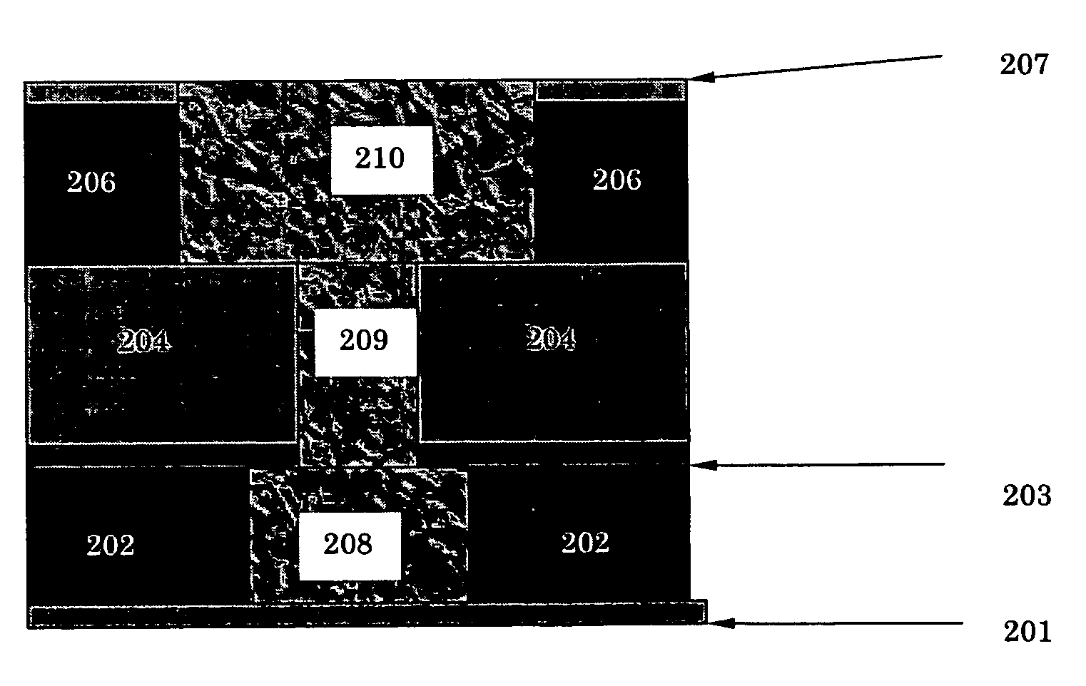
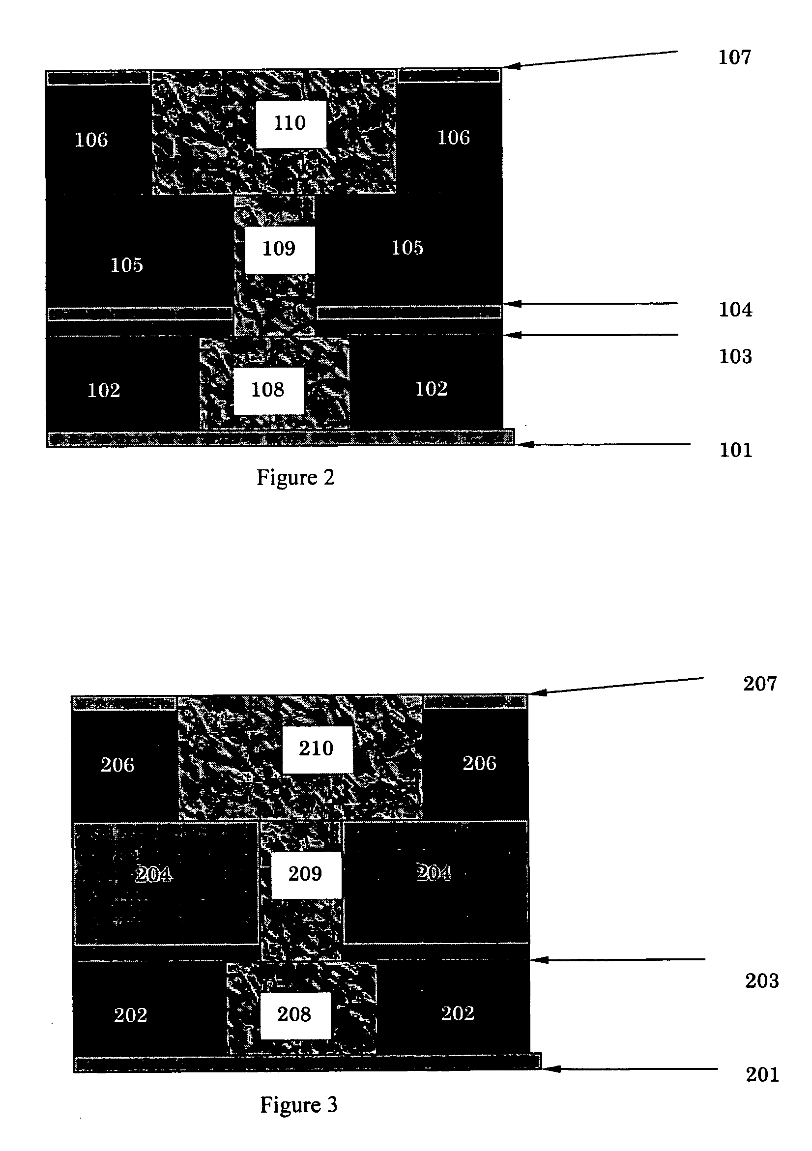
[0039] In an embodiment, the present invention concerns applying organosillicate layers as a cap on top of a via and dual hard layers at a bottom of the via in copper dual damascene structures. In a specific embodiment, the thickness of the cap layer 107 may be between about 50 nm and about 100 nm. In an embodiment, the thickness of the etch stop layer 103 may range from 10 nm to 200 nm. The thickness of the bottom layer 104 can vary up to the height of a via 109. That is, the layer 104 can replace the layer 105 entirely. Thus, in an embodiment, the thickness of the layer 104 may range from about 10 nm to about 500 nm. In the figures, the layers 207 and 307 correspond to the layer 107, the layers 203 and 303 co...


PUM


Abstract

A method of forming an interconnect for a semiconductor device using triple hard layers, comprises: forming a first hard layer serving as an etch stop layer on a metal interconnect-formed dielectric layer; forming a second hard layer on the first hard layer; forming a dielectric layer on the second hard layer; forming a third hard layer on the dielectric layer; forming a hole through the third and second hard layers, the dielectric layer, and the first hard layer; and filling the hole with metal to establish an interconnect. The second and third hard layers are each made of carbon-doped silicon oxide formed from a source gas and a redox gas, while controlling the carbon content in the second hard layer as a function of a flow rate of the redox gas.

Description

BACKGROUND OF THE INVENTION [0001] 1. Field of the Invention [0002] The present invention relates to a carbon-doped silicon oxide film and a damascene structure using the same, and in particular, to a low-carbon-doped silicon oxide film formed with a redox gas, and a damascene structure using dual hard films constituted by the low-carbon-doped silicon oxide. [0003] 2. Description of the Related Art [0004] Integrated circuits have evolved into complicated devices that include various components. (e.g., SRAM (static random access memory) transistor, MIM (metal insulator metal), RFIC (radio frequency integrated circuit) and logic circuits on a single chip. The evolution of chip designs demands a continuous improvement on circuit speed and reliability. Hence, this give rises to a need to compact the devices into higher packing density to achieve faster transistor speed. Nevertheless, down sizing of the devices is not always preferable for chipmakers. Increasing in density up to the sub ...

Claims


Application Information

Patent Timeline
IPC IPC(8): H01L21/316H01L21/768H01L21/4763H01L23/532
CPCH01L21/76807H01L21/76832H01L21/76834H01L23/53238H01L23/5329H01L2924/0002H01L23/53295H01L2924/00
Inventor LOKE, CHOU SAN NELSONYOSHIOKA, KANAKOSATOH, KIYOSHI
Owner ASM JAPAN
Why Eureka
Try Eureka