[0008] It is, therefore, an object of the present invention to provide a plasma processing apparatus and a mounting unit thereof capable of accurately detecting a substrate's temperature by reducing an effect that an
electric field or
magnetic field generated by supplying a
high frequency power to power feed path members has on detection of the substrate's temperature.
[0014] In accordance with the present invention, a temperature detection unit formed of a
dielectric material, power feed path members for supplying a high frequency
voltage to the mounting table, and conductive path members for supplying a power to the heating unit are provided in a protection
pipe having one end portion disposed at the mounting table, wherein the power feed rods and the conductive path members are disposed such that the region having therein the temperature detection unit is an electromagnetic wave-free region where electromagnetic
waves traveling from the power feed rods to the conductive path members are offset with each other. Consequently,
dielectric heating caused by electromagnetic
waves is suppressed in the temperature detection unit formed of a dielectric material, thereby reducing a
noise component caused by heating in a detected temperature value. As a result, the temperature of substrate can be precisely measured and a favorable process can be performed on the substrate.
[0015] Further, similarly in a case that the temperature detection unit is formed of a conductive material, a
magnetic field generated around one power feed path member becomes weakened by a magnetic field generated around the other power feed path member. Accordingly, in this case, magnetic
force lines generated in the region having therein temperature detection unit become weaker than those generated when only one power feed path member is provided. As a result, generation of
induction heating is suppressed in the temperature detection unit, thereby reducing a
noise component caused by heating in a detected temperature value. DETAILED DESCRIPTION OF THE PREFERRED EMBODIMENTS
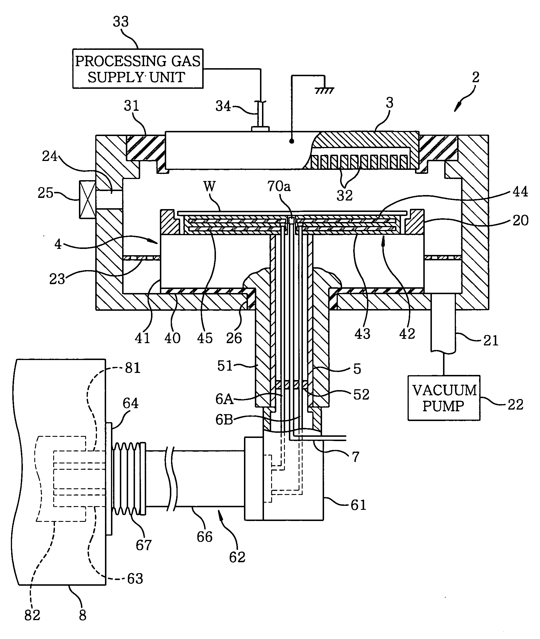
[0030] Therefore, one portion of the cylindrical part 66, e.g., the cylindrical part 66's leading end portion connected to the
flange portion 64, is formed of a
bellows member 67 in this embodiment. Accordingly, the
bellows member 67 can accommodate the misalignment in the above position relationship, thereby relieving load stress applied to the cylindrical part 66 and the power feed paths when attaching or detaching the second power feed path unit 62, so that attachment or detachment thereof becomes easy.
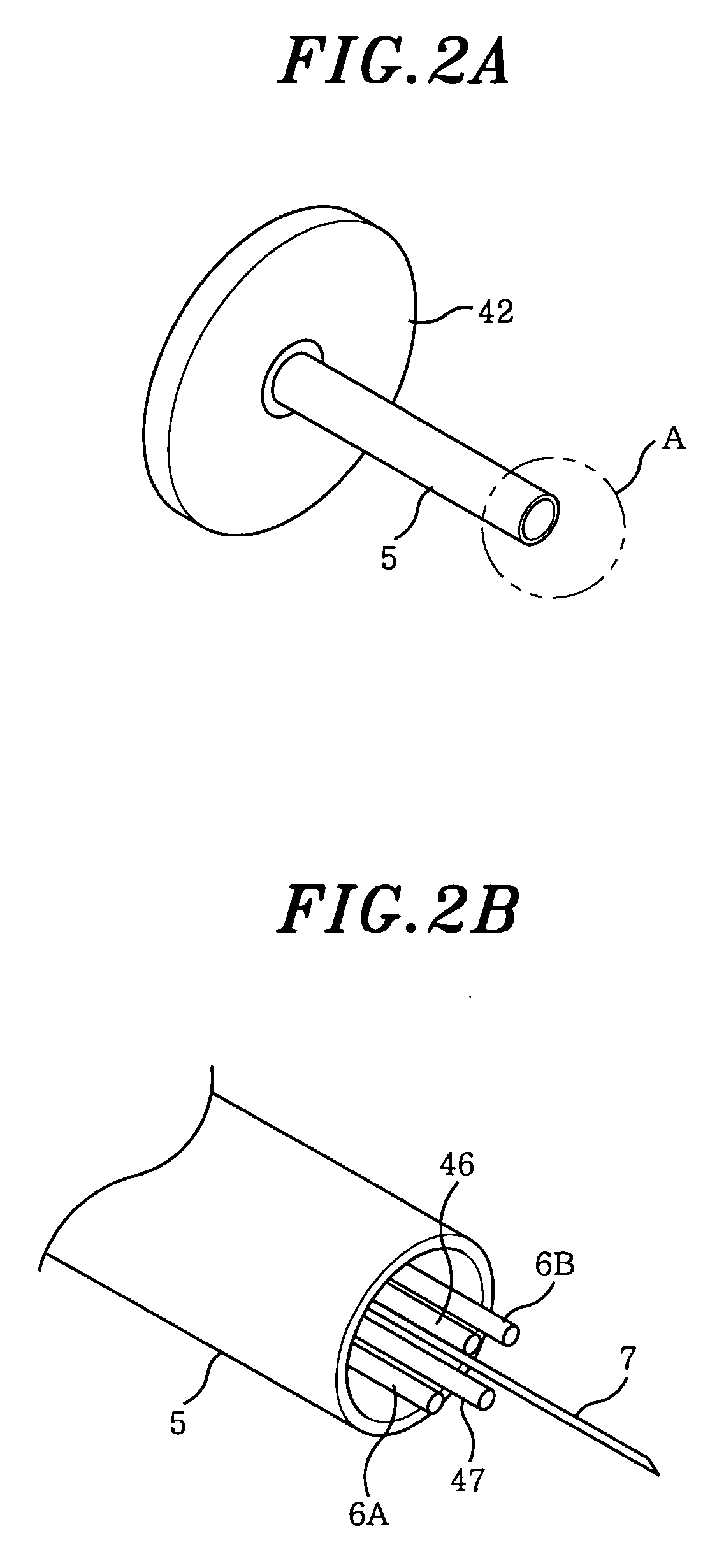
[0035] Additionally, when high frequency current flows in the RF feed rods 6A and 6B, the bar type conductive leads 46 and 47 to be used for applying a
DC voltage practically function as if they are grounded with respect to the high frequency current, thereby forming an
electric field where electromagnetic
waves travel from the RF feed rods 6A and 6B to the bar type conductive leads 46 and 47, respectively. Here, the RF feed rods 6A and 6B and the bar type conductive leads 46 and 47 are alternately arranged at equal intervals (divided into four parts) in a circumferential direction on a circle having the optical
fiber 7 at the center thereof. Accordingly, as shown in FIG. 7, vectors of
electric force lines originating from the RF feed rods 6A and 6B become zero in theory. Namely, the region having therein the optical
fiber 7, specifically, the fluorescent material 70 that is a dielectric material disposed at the leading end of the optical fiber 7, is an electromagnetic wave-free region since the electromagnetic waves respectively traveling from the RF feed rods 6A and 6B to the bar type conductive leads 46 and 47 are offset with each other. Consequently, the
dielectric heating is suppressed in the fluorescent material 70 and the fluorescent material 70 is heated to the temperature corresponding to the
wafer's temperature. As a result, the temperature of the
wafer W can be precisely measured and a favorable process can be performed.
[0036] Further, a magnetic field is generated around the RF feed rods 6A and 6B due to the high frequency current flowing therein, and an
eddy current is generated in the protection cap 70a made of a conductive material such as aluminum. However, the protection cap 70a is placed at the midpoint of a line that links the two RF feed rods 6A and 6B, and magnetic
force lines MA and MB whose magnitudes are same in theory are generated, e.g.,
clockwise around the respective RF feed rods 6A and 6B as shown in FIG. 7. Accordingly, the effects of magnetic
force lines MA and MB are offset with each other at an arbitrary point of time at the region of the protection cap 70a. As a result, generation of an
eddy current is suppressed at the protection cap 70a and an
induction heating level is low, whereby the temperature can be further precisely detected.

