Semiconductor device with strain

a technology of semiconductor and strain, which is applied in the direction of semiconductor devices, semiconductor/solid-state device details, electrical apparatus, etc., can solve the problems of inability to improve the performance of the whole cmos, and the difficulty of further miniaturization of mosfets, so as to achieve the effect of improving the performance of mosfets

Active Publication Date: 2005-12-29
TRINITY SEMICON RES
View PDF7 Cites 76 Cited by
  • Summary
  • Abstract
  • Description
  • Claims
  • Application Information

AI Technical Summary

Benefits of technology

[0022] The performance of MOSFET can be improved by stress along the gate length direction and gate width direction exerted on the channel region.

Problems solved by technology

The requested minimum patterning size has become recently a size smaller than the wavelength of light used by lithography, and further miniaturization of MOSFETs is becoming difficult.
As described above, as the inner stress of a contact etch stopper film is increased, the on-current increases in one of an n-MOSFET and a p-MOSFET and decreases in the other so that the increase and decrease are canceled out and there is the tendency that the performance of the whole CMOS cannot be improved.

Method used


Image

  • Semiconductor device with strain
  • Semiconductor device with strain
  • Semiconductor device with strain

Examples


first embodiment

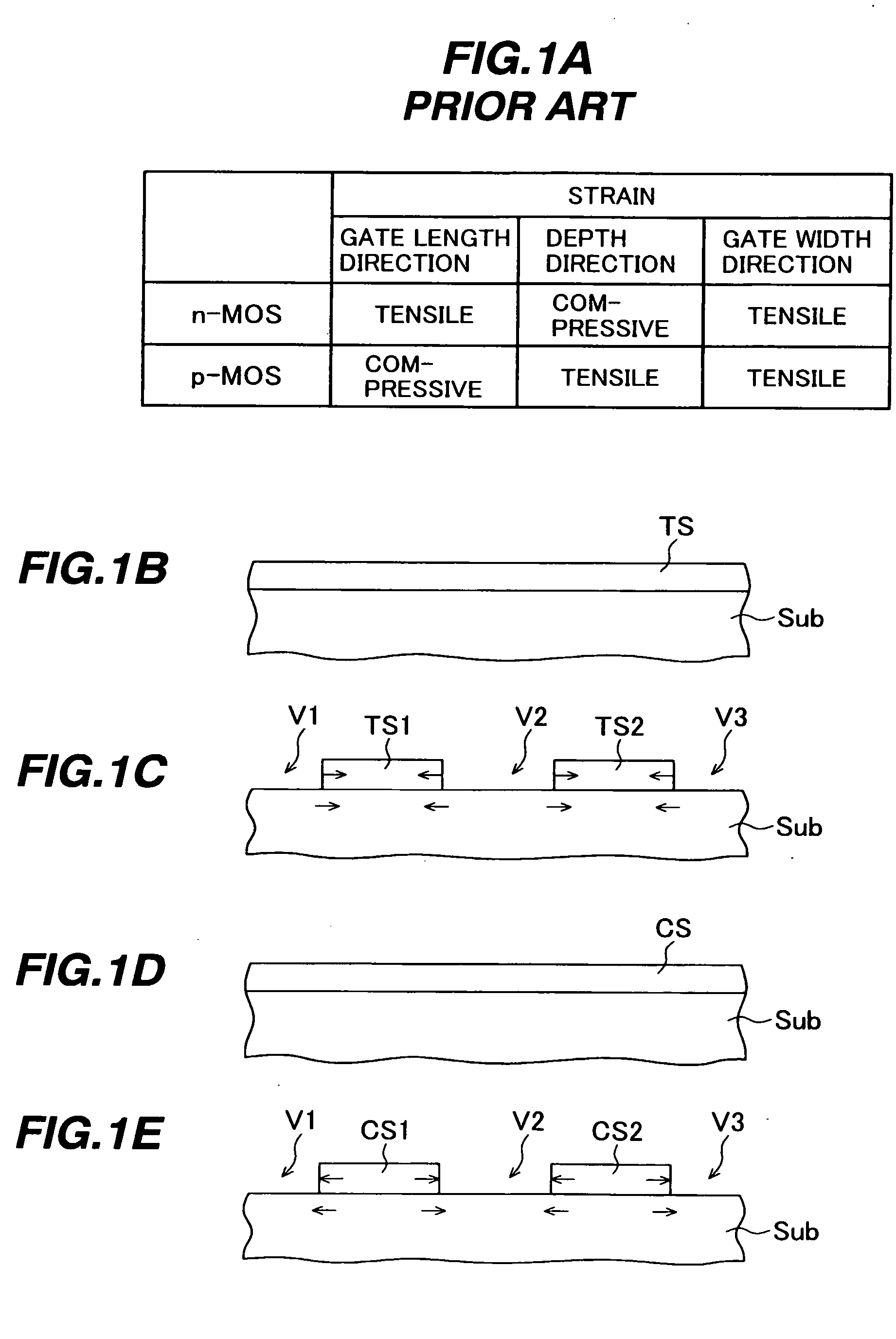
[0067]FIGS. 5A to 5D are cross sectional views and a plan view showing a CMOS structure according to the As shown in FIG. 5A, a trench is formed in the surface layer of a (001) plane p-type silicon substrate, an insulating layer is buried in the trench and thereafter an unnecessary region is removed to form an element isolation region 12 defining active regions by shallow trench isolation (STI). Impurities of p- and n-types are selectively implanted to form a desired p-well 13 and n-well 14. The surface of the active region is thermally oxidized and if necessary nitridized to form a gate insulating film 15.

[0068] A polysilicon layer is deposited on the gate insulating film to a thickness of, e.g., about 100 nm to form a gate electrode layer. By using a resist pattern, the gate electrode layer and gate insulating film are patterned to form an insulated gate electrode G (collectively indicating Gn and Gp) having a gate length of, e.g., 50 nm along the direction. Impurities of n- and...

second embodiment

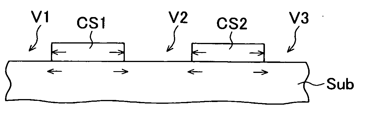
[0082] In the second embodiment, a silicon nitride film 21 having a tensile stress is formed in the n-MOS region and a silicon nitride film 32 having a compressive stress is formed in the p-MOS region.

[0083] The silicon nitride film 32 having a compressive stress is deposited on the silicon substrate, covering the insulated gate electrodes Gn and Gp. For example, the silicon nitride film 32 having the compressive stress of about 1.4 GPa is deposited to a thickness of about 80 nm by PECVD under the conditions that SiH4 is flowed at 100 to 1000 sccm as silicon source gas, NH3 is flowed at 500 to 10000 sccm as nitrogen source gas, and Ar+N2 are flowed at 500 to 10000 sccm as other gasses, at a pressure of 0.1 to 400 torr and an RF power of 100 to 1000 W.

[0084] By covering the p-MOS region with a resist pattern, the compressive stress silicon nitride film 32 in the n-MOS region is removed. Next, the silicon nitride film 21 having a thickness of about 80 nm and a tensile stress of 1.4 G...

fourth embodiment

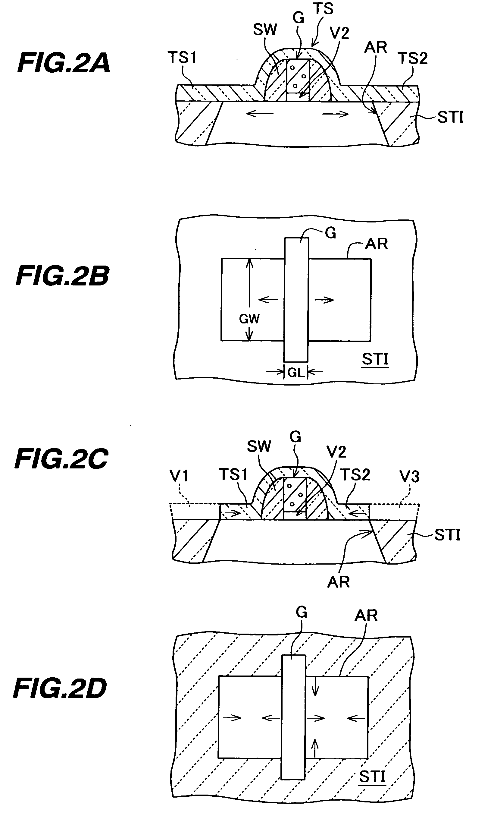
[0097]FIGS. 10A to 10D are schematic cross sectional views and a plan view showing the structure of a semiconductor device of the fourth embodiment and its main manufacture processes.

[0098] As shown in FIG. 10A, an n-MOSFET and a p-MOSFET are formed on a semiconductor substrate 11 by the processes similar to those of the above-described embodiments. A contact etch stopper film 32 of a silicon nitride film having a compressive stress is formed on the semiconductor substrate.

[0099]FIG. 10B is a plan view of the semiconductor substrate as viewed from the upper position. An element isolation region 12 by STI defines an n-MOS active region AR1 and a p-MOS active region AR2. Gate electrode structures Gn and Gp are formed traversing the active regions AR1 and AR2.

[0100] As shown in FIG. 10C, a compressive stress film 32 is formed on the whole surface of the semiconductor substrate, covering the gate electrode structures. A resist pattern is formed on the compressive stress film 32. The r...


PUM


Abstract

A semiconductor device includes: a semiconductor substrate having a p-MOS region; an element isolation region formed in a surface portion of the semiconductor substrate and defining p-MOS active regions in the p-MOS region; a p-MOS gate electrode structure formed above the semiconductor substrate, traversing the p-MOS active region and defining a p-MOS channel region under the p-MOS gate electrode structure; a compressive stress film selectively formed above the p-MOS active region and covering the p-MOS gate electrode structure; and a stress released region selectively formed above the element isolation region in the p-MOS region and releasing stress in the compressive stress film, wherein a compressive stress along the gate length direction and a tensile stress along the gate width direction are exerted on the p-MOS channel region. The performance of the semiconductor device can be improved by controlling the stress separately for the active region and element isolation region.

Description

CROSS REFERENCE TO RELATED APPLICATION [0001] This application is based on and claims priority of Japanese Patent Application No. 2004-191405 filed on Jun. 29, 2004, the entire contents of which are incorporated herein by reference. BACKGROUND OF THE INVENTION [0002] A) Field of the Invention [0003] The present invention relates to a semiconductor device, and more particularly to a semiconductor device having a contact etch stopper film having stress therein and formed above a semiconductor substrate. [0004] B) Description of the Related Art [0005] There are high demands for high integration and high speed of semiconductor integrated circuit devices. High integration and high speed have been achieved conventionally by reducing the size of a MOS field effect transistor (FET) which is a main constituent element of a semiconductor integrated circuit device. Miniaturization can obviously improve the integration degree and a shortened gate length can increase an operation speed. Miniatur...

Claims


Application Information

Patent Timeline
Patent Type & Authority Applications(United States)
IPC IPC(8): H01L21/3115H01L21/8238H01L29/73
CPCH01L21/31155H01L21/823807H01L21/823828H01L29/7843H01L2924/0002H01L2924/00
Inventor SATOH, SHIGEO
Owner TRINITY SEMICON RES
Why Eureka
Try Eureka