Semiconductor device and semiconductor signal processing apparatus

a semiconductor signal and semiconductor technology, applied in the field of semiconductor devices, can solve the problems of insufficient dedicated dsp to achieve dramatic improvement in performance, limited address area available for data reading and writing by each logic module accessing multi-port data memory, and insufficient data reading and writing to achieve the effect of dramatic improvement in performan

Inactive Publication Date: 2005-12-29
RENESAS ELECTRONICS CORP
View PDF2 Cites 164 Cited by
  • Summary
  • Abstract
  • Description
  • Claims
  • Application Information

AI Technical Summary

Benefits of technology

[0035] As the processor and a register are arranged in the processing circuit, it becomes possible to execute various arithmetic/logic operations in the bit-serial manner, by storing the data as the object of arithmetic/logic operation in the register.
[0036] Further, by providing a plurality of register circuits in the processing circuit, multiplication in accordance with second-order Booth's algorithm becomes possible, even when multiplication is performed in the bit-serial manner.
[0037] Further, by transmitting a control signal commonly to every prescribed number of operation blocks among the operation blocks, an arithmetic/logic operation required by the unit of a prescribed number of operation blocks can be executed. Consequently, operation control becomes easier than in an arrangement in which each of the operation blocks is controlled individually, and a plurality of data can be processed

Problems solved by technology

Therefore, an address area available for data reading and writing by each logic module accessing the multi-port data memory is limited.
When the amount of data to be processed is very large, even a dedicated DSP is insufficient to attain dramatic improvement in performance.
Therefore, though each process can be done at high speed in an arrangement that performs the sum-of-products operation using a register file such as described in Reference 1, when the amount of data increases, the time of processing increases in proportion thereto as the data are processed in series, and therefore, such an arrangement cannot achieve high speed processing.
When such a dedicated DSP is used, the processing performance greatly depends on operating frequency, and therefore, if high speed processing were given priority, power consumption would considerably be increased.
When the arrangement is to be diverted to another application, the bit width, configuration of processing circuit and others be re-designed, and hence

Method used


Image

  • Semiconductor device and semiconductor signal processing apparatus
  • Semiconductor device and semiconductor signal processing apparatus
  • Semiconductor device and semiconductor signal processing apparatus

Examples


embodiment 1

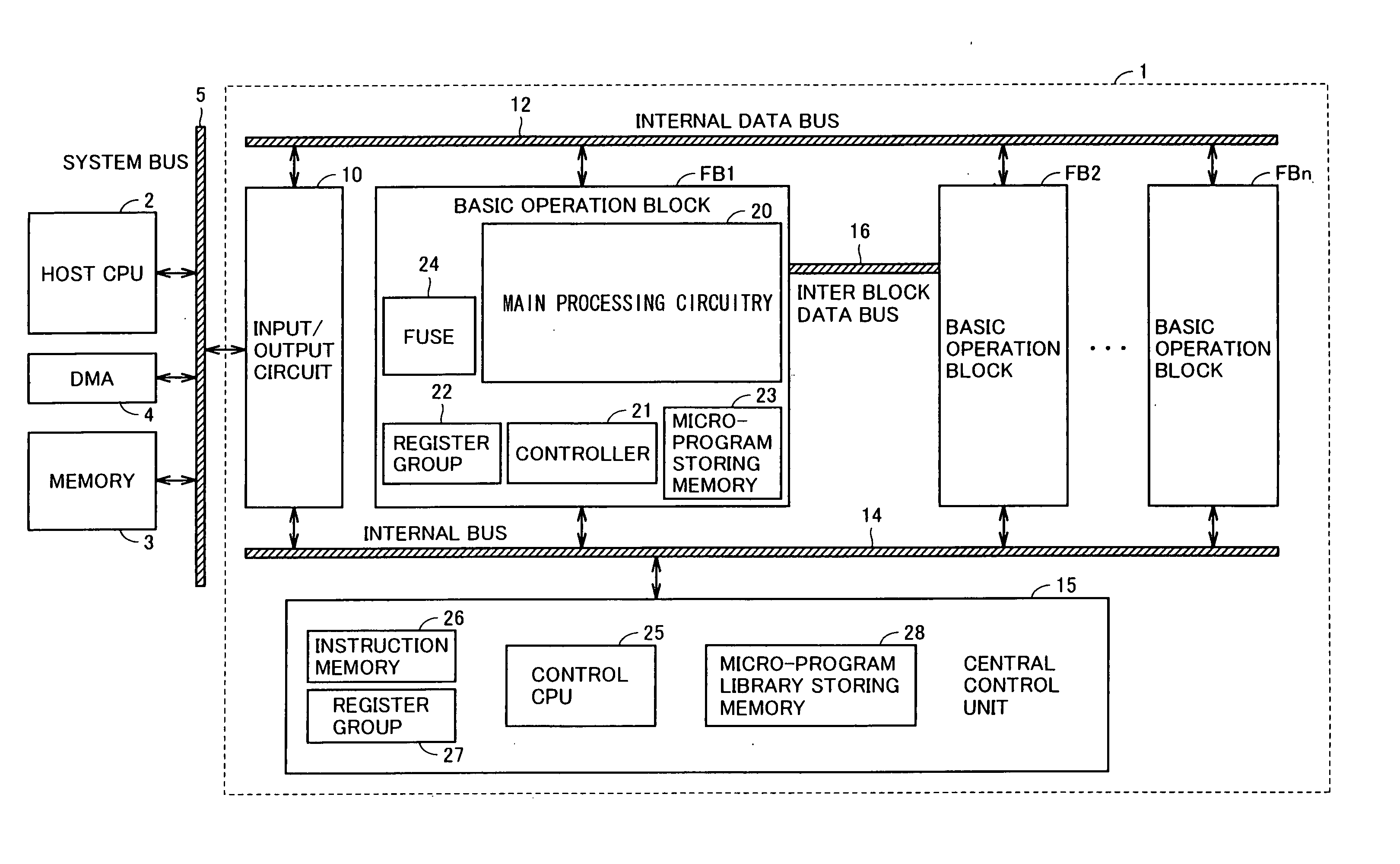
[0184]FIG. 1 schematically shows configuration of a processing system utilizing a semiconductor processing device in accordance with Embodiment 1 of the present invention. Referring to FIG. 1, the processing system includes a semiconductor processing device 1; a host CPU 2 performing process control in semiconductor processing device 1, control of the system as a whole and data processing; a memory 3 used as a main storage of the system and storing various necessary data; and a DMA (Direct Memory Access) circuit 4 directly accessing memory 3 without communication through host CPU 2. By the control of DMA circuit 4, data can be transferred between memory 3 and semiconductor processing device 1, and semiconductor processing device can be accessed directly.

[0185] Host CPU 2, memory 3, DMA circuit 4 and semiconductor processing device 1 are connected to each other through a system bus 5. Semiconductor processing device 1 includes a plurality of basic operation blocks FB1 to FBn provide...

embodiment 2

[0246]FIG. 10 shows a structure of a memory cell MC of the memory mat in accordance with Embodiment 2 of the present invention. Referring to FIG. 10, memory cell MC is a dual port memory cell having a write port and a read port provided separately. For the memory cell MC, a read word line RWL and a write word line WWL, as well as read bit lines RBL and / RBL and write bit lines WBL and / WBL are provided. The read port includes N channel MOS transistors NQ5 and NQ6 connecting storage nodes SN1 and SN2 to read bit lines RBL and / RBL, respectively, in response to a signal potential of read word line RWL. The write port includes N channel MOS transistors NQ7 and NQ8 connecting storage nodes SN1 and SN2 to write bit lines WBL and / WBL, respectively, in response to a signal potential of read word line WWL.

[0247] A data storage portion of memory cell MC includes load P channel MOS transistors PQ1 and PQ2 as well as driving N channel MOS transistors NQ1 and NQ2.

[0248] By using the dual por...

embodiment 3

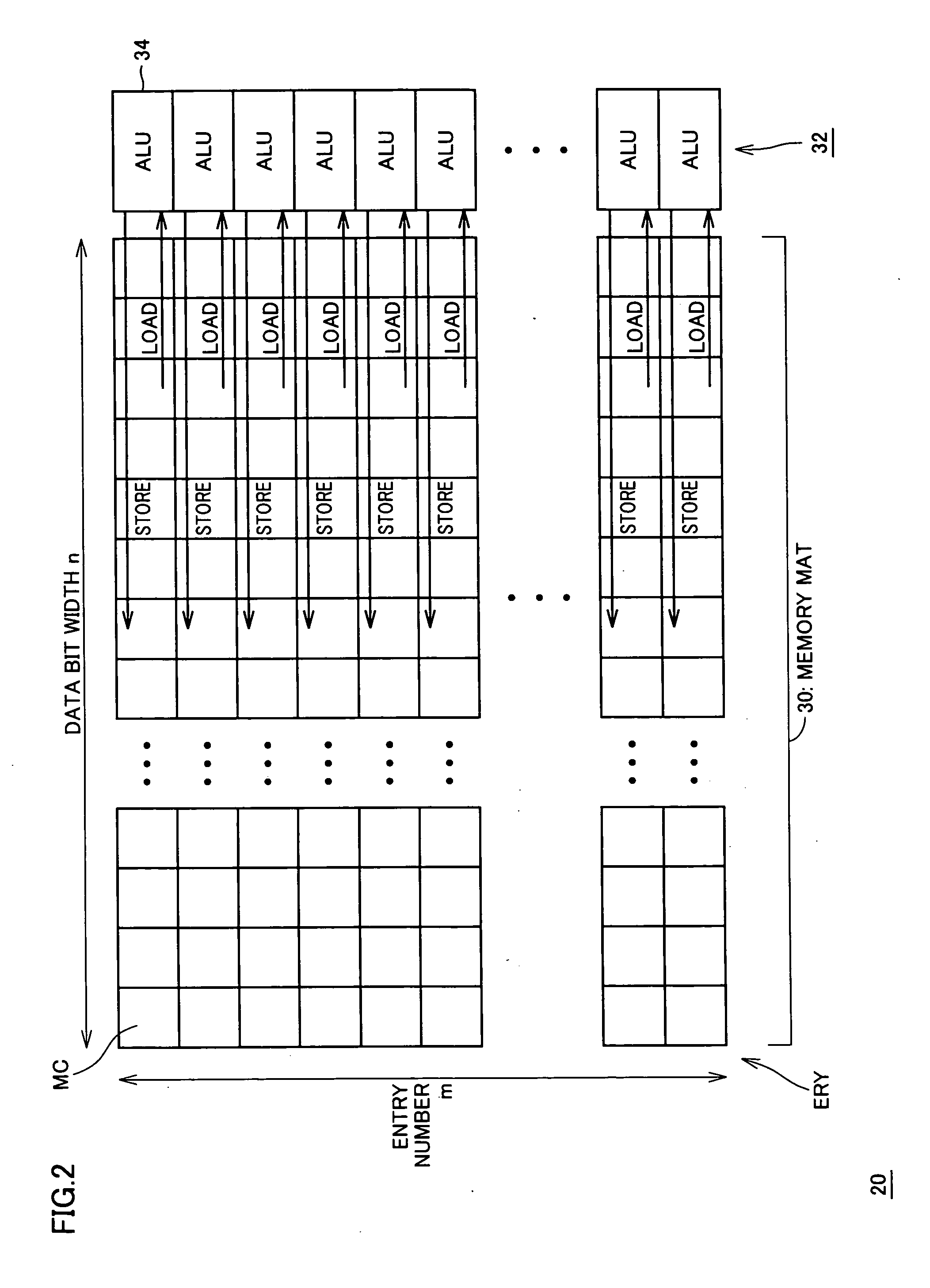
[0267]FIG. 13 schematically shows a configuration of a main portion of main processing circuitry 20 in accordance with Embodiment 3 of the present invention. In main processing circuitry 20 shown in FIG. 13, memory mats 30A and 30B are arranged on both sides of the group of arithmetic logic units 32. Memory mats 30A and 30B are of the same structure, each having m entries ERY of which data width is n bits. Between each entry of memory mats 30A and 30B, ALU 34 of the group of arithmetic logic units 32 is arranged. ALU 34 performs a designated arithmetic / logic operation on the data of the corresponding entries of memory mats 30A and 30B. When each ALU34 is to perform a two term operation, data to be processed for each term are stored in memory mats 30A and 30B, and the result of operation is stored in one of memory mats 30A and 30B. Therefore, in memory mats 30A and 30B, the amount of data to be stored can be reduced as compared with a configuration utilizing only one memory mat. The ...


PUM


Abstract

A memory cell mat is divided into a plurality of entries, and an arithmetic logic unit is arranged corresponding to each entry. Between the entries and the corresponding arithmetic logic units, arithmetic/logic operation is executed in bit-serial and entry-parallel manner. Where parallel operation is not very effective, data is transferred in entry-serial and bit-parallel manner to a group of processors provided at a lower portion of the memory mat. In this manner, a large amount of data can be processed at high speed regardless of the contents of operation or data bit width.

Description

BACKGROUND OF THE INVENTION [0001] 1. Field of the Invention [0002] The present invention relates to a semiconductor device and, more specifically, to a configuration of a processing circuit using a semiconductor memory performing arithmetic / logic operation on a large amount of data at high speed. [0003] 2. Description of the Background Art [0004] Recently, along with wide spread use of portable terminal devices, digital signal processing allowing high speed processing of a large amount of data including voice and image comes to have higher importance. For such digital signal processing, generally, a DSP (Digital Signal Processor) is used as a dedicated semiconductor device. Digital signal processing of audio and image includes data processing such as filtering, which frequently requires arithmetic operations with repetitive product and sum operations. Therefore, a DSP is generally configured to contain a multiplication circuit, an adder circuit and a register for accumulation. When...

Claims


Application Information

Patent Timeline
IPC IPC(8): G06F15/16G11C7/10
CPCG11C7/1006
Inventor NODA, HIDEYUKISAITOH, KAZUNORIARIOMOTO, KAZUTAMIDOSAKA, KATSUMI
Owner RENESAS ELECTRONICS CORP
Why Eureka
Try Eureka