Semiconductor device and method for manufacturing same

a semiconductor and film technology, applied in semiconductor devices, capacitors, electrical equipment, etc., can solve the problems of difficult manufacturing of cmos (complementary mos), metals cannot be practically employed, and the gate insulating film is easily short-circuited, so as to prevent the occurrence of a grain boundary passing through the insulating film, the effect of suppressing the crystallization of hafnium oxide and preventing the lowering of electrostatic capacitan

Inactive Publication Date: 2006-01-05
RENESAS ELECTRONICS CORP
View PDF4 Cites 8 Cited by
  • Summary
  • Abstract
  • Description
  • Claims
  • Application Information

AI Technical Summary

Benefits of technology

[0010] In view of the above, it is an object of the present invention to provide a semiconductor device which is capable of improving its reliability, even when a polycrystalline semiconductor such as a polycrystalline silicon or a like is used as a material for its gate electrode, by using a material having a high relative dielectric constant for a gate insulating film, by suppressing degradation of an EOT and by preventing crystallization of the material having a high relative dielectric constant, and a method for manufacturing the same.
[0039] With still another configuration, the concentration of aluminum is set to be comparatively high in a region having a specified thickness immediately below the electrode and, therefore, by using a polycrystalline semiconductor as a gate electrode, lowering in an EOT of the insulating film occurring when hafnium oxide is singly used as the insulating film can be suppressed, which enables electrostatic capacitance to be prevented from being lowered.
[0040] With still another configuration, aluminum is contained not only in the second insulating region but also in the first insulating region where hafnium is contained in a comparatively high concentration and, therefore, crystallization of hafnium oxide can be suppressed. As a result, occurrence of a grain boundary passing through the insulating film can be suppressed and an increase in leakage currents can be prevented. This enables dielectric breakdown to be avoided and reliability of semiconductor devices to be improved. Thus, since the crystallization of hafnium oxide can be suppressed, it is possible to improve surface roughness and to avoid local concentration of electric fields at regions having small thickness and to reduce leakage currents, which improve reliability of semiconductor devices.
[0041] With still another configuration, after the second insulating region has been stacked on the first insulating film, by performing the thermal treatment process, the concentrations of aluminum and hafnium can be changed continuously and, therefore, it is possible to prevent such a problem as a decrease in a threshold value caused by trapped electric charges in the boundary region.
[0042] With still another configuration, the ALD method is used to form the insulating film and, therefore, the concentration of aluminum and hafnium can be precisely controlled, thus improving quality of the insulating film and contamination caused by carbon contained in the material gas can be prevented by introducing the purge gas.

Problems solved by technology

However, a problem arises that, if the gate insulating film is made so extremely thin, a tunnel current flowing when a gate bias is applied becomes so large, compared with a source-drain current, that it cannot be neglected.
Moreover, when metals as described above are used as the materials for the gate electrode 205, though an experiment on only such the characteristic as the relation between the EOT and leakage current density shows good results, the metals cannot be practically employed due to following reasons.
However, if metals are used as the material for the gate electrode, since a work function cannot be changed, there is a difficulty in manufacturing a CMOS (Complementary MOS).
Also, generally, if metals are used as a material for the gate electrode, the gate insulating film is easily short-circuited due to a reaction between the gate electrode and gate insulating film caused by heat treatment for source / drain activation.
However, this method has also a problem in that, if zirconium oxide is used as the material for the gate insulating film, crystallization of amorphous zirconium oxide occurs due to heat treatment in a process of forming the gate electrode 105 or of forming the source / drain region 102, or if polycrystalline silicon is used as the material for the gate electrode 105, a short-circuit is made due to incompatibility with zirconium oxide.
Moreover, an another problem arises that, if hafnium oxide is used as the material for the gate insulating film, crystallization of the hafnium oxide easily occurs due to heat treatment which causes occurrence of a grain boundary passing through higher and lower electrodes.
These problems cause an increase in a leakage current leading to easy occurrence of dielectric breakdown and to reduction in reliability of semiconductor devices.

Method used


Image

  • Semiconductor device and method for manufacturing same
  • Semiconductor device and method for manufacturing same
  • Semiconductor device and method for manufacturing same

Examples


first embodiment

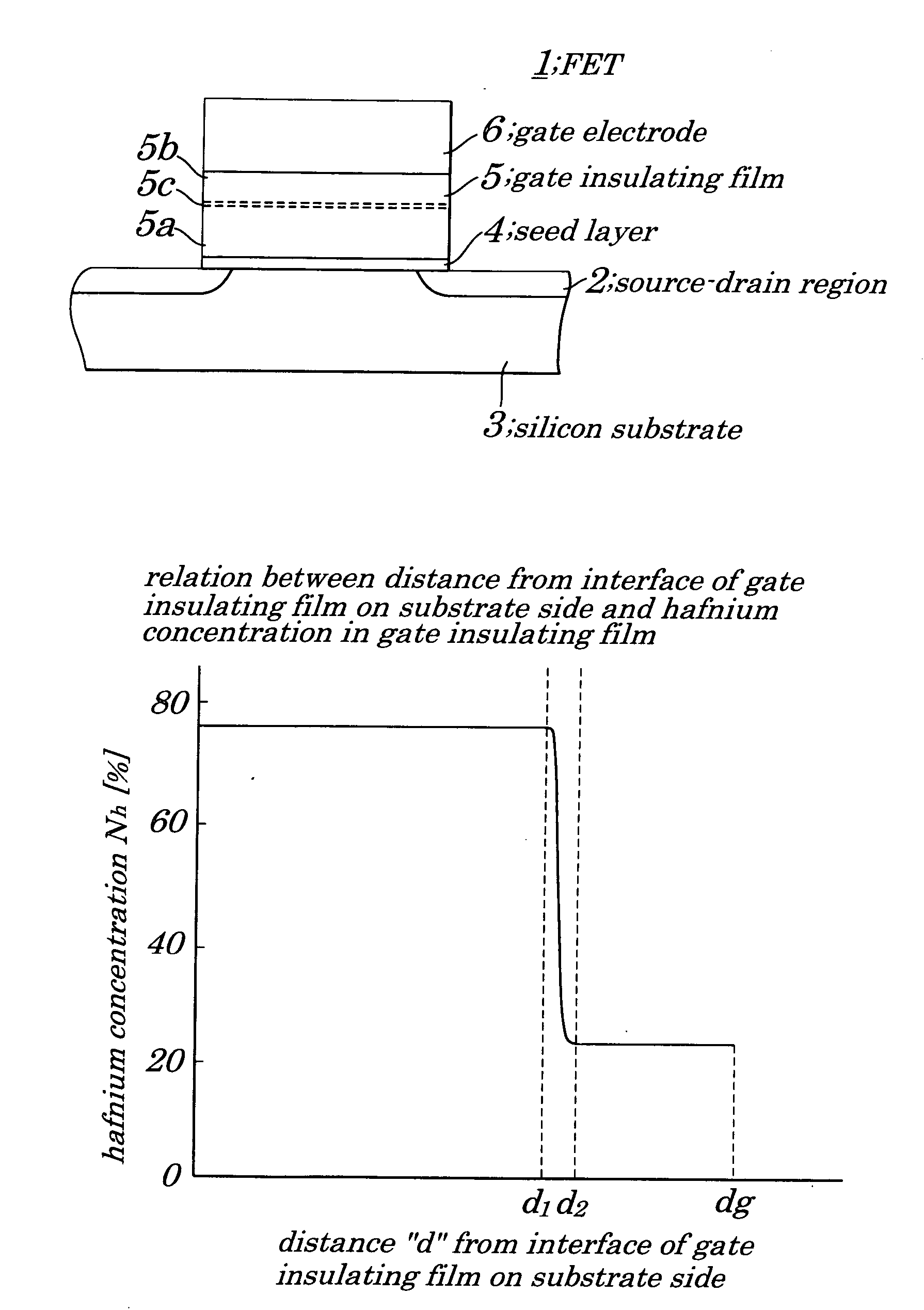
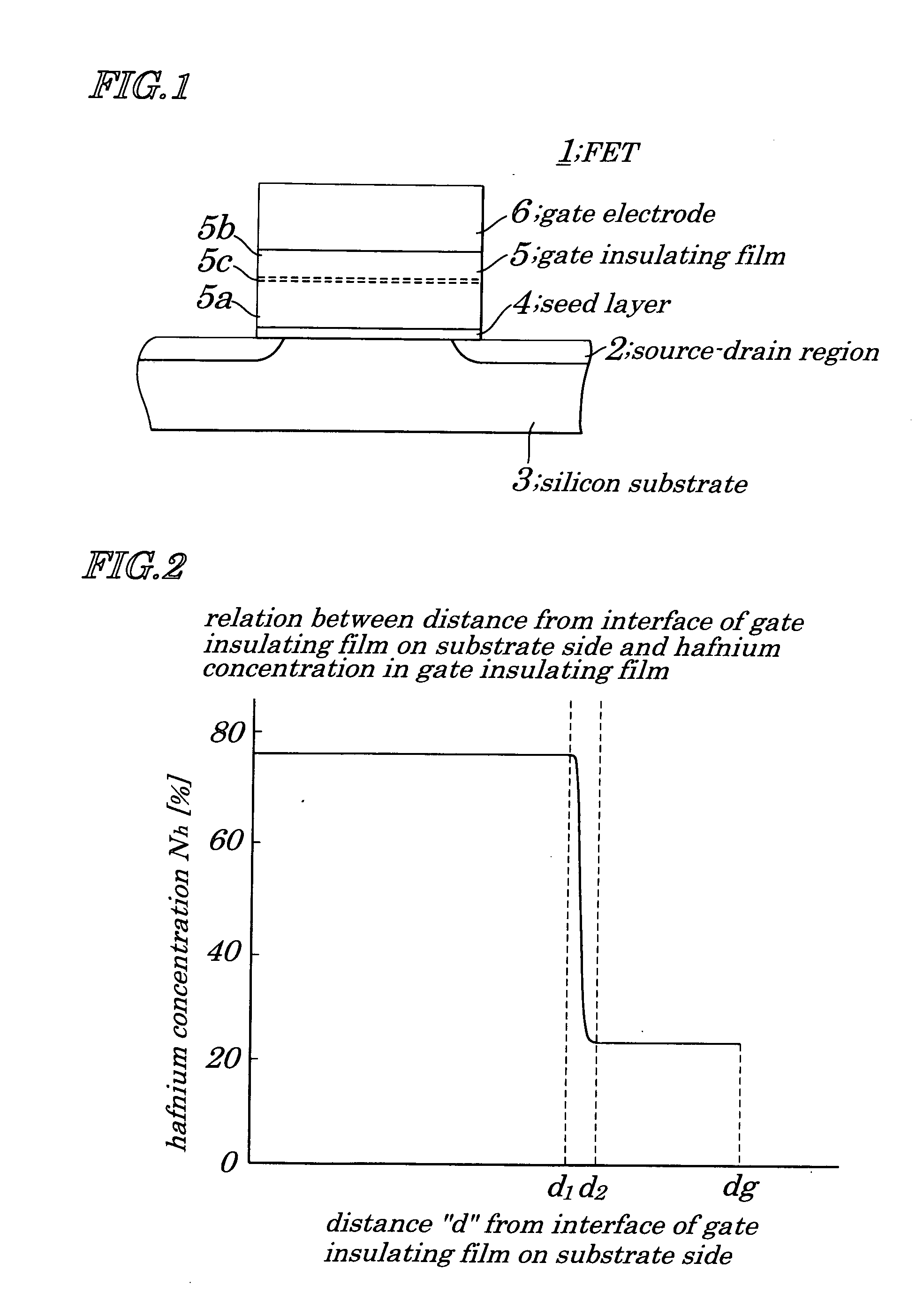
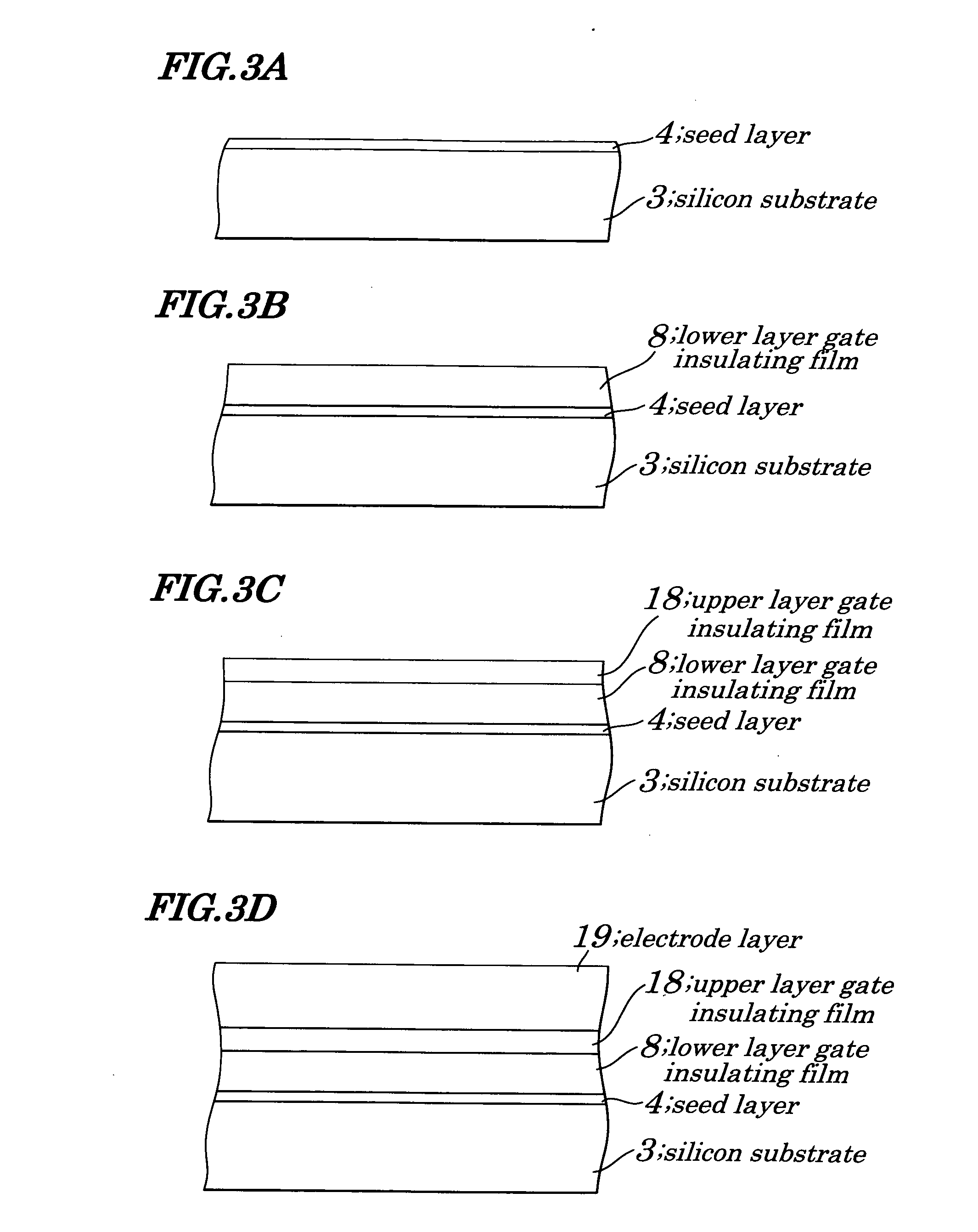
[0062]FIG. 1 is a cross-sectional view for schematically illustrating featured configurations of an FET (Field Effect Transistor) according to a first embodiment of the present invention. FIG. 2 is a characteristic diagram briefly showing a relation between a distance from an interface of a gate insulating film on a side of a substrate and a hafnium concentration “Nh” obtained after heat treatment in a gate insulating film making up the FET according to the first embodiment. FIGS. 3A to 3D, and FIGS. 4A and 4B are process diagrams for illustrating a method for manufacturing the FET according to the first embodiment. FIG. 5 is a diagram briefly showing an ALD (Atomic-Layer Deposition) system to be used for manufacturing the FET according to the first embodiment. FIG. 6 is a diagram explaining a method for supplying material gas or a like employed in the ALD system of FIG. 5. FIG. 7 is a diagram explaining a method for supplying material gas or a like employed in the ALD system of FIG...

second embodiment

[0085]FIG. 10 is a cross-sectional view for schematically illustrating configurations of main portions of an FET according to a second embodiment of the present invention. FIG. 11 is a cross-sectional view schematically illustrating configurations of intermediate regions in a gate insulating film of the FET 21 of the second embodiment. FIG. 12 is a characteristic diagram briefly showing a relation between a distance from an interface of the gate insulating film on a substrate side in the gate insulating film making up the FET 21 and a hafnium concentration “Nh” obtained after heat treatment in the gate insulating film making up the FET 21 of FIG. 10. FIGS. 13A, 13B and 13C are process diagrams illustrating a method for manufacturing the FET 21 of FIG. 10. FIG. 14 is a characteristic diagram briefly showing a relation between a distance from the interface of the gate insulating film on the substrate side in the gate insulating film making up the FET 21 and a hafnium concentration “Nh...


PUM

PropertyMeasurementUnit
thicknessaaaaaaaaaa
thicknessaaaaaaaaaa
relative dielectric constant εraaaaaaaaaa

Abstract

A semiconductor device is provided which is capable of improving its reliability by using a material having a high relative dielectric constant as a material for its gate insulating film, by suppressing degradation of an EOT (Equivalent Oxide Thickness) and by preventing crystallization of the material having a high relative dielectric constant. The semiconductor device (Field Effect Transistor) has a silicon substrate, a seed layer made up of silicon oxide, a gate insulating film made of amorphous hafnium aliminate and a gate electrode made up of polycrystalline silicon formed the gate insulating film. The gate insulating film is so formed that a hafnium concentration decreases monotonously or step by step, whereas an aluminum concentration increases monotonously or step by step along a direction of a thickness of the gate insulating film from the silicon substrate side toward the gate electrode. In a boundary region between a lower layer side region and an upper layer side region in the gate insulating film, the hafnium and aluminum concentrations change continuously.

Description

BACKGROUND OF THE INVENTION [0001] 1. Field of the Invention [0002] The present invention relates to a semiconductor device and a method for manufacturing the same, and more particularly to an MIS (Metal Insulator Semiconductor)-type semiconductor device in which a gate electrode made of, for example, polycrystalline silicon is formed on a silicon substrate with a gate insulating film made of amorphous aluminate, and being sandwiched between the gate electrode and the silicon substrate, and to the method for manufacturing the same. [0003] The present application claims priority of Japanese Patent Application No. 2002-381216 filed on Dec. 27, 2002, which is hereby incorporated by reference. [0004] 2. Description of the Related Art [0005] In recent years, to satisfy a need for scale-down and high integration of a semiconductor device, when silicon oxide (SiO2) is used as a gate insulating film, it is necessary to reduce its film thickness of, for example, an FET (Field Effect Transist...

Claims


Application Information

Patent Timeline
Patent Type & Authority Applications(United States)
IPC IPC(8): H01L21/469H01L21/31H01L21/4763H01L21/3205H01L21/316H01L21/02H01L21/28H01L21/314H01L29/51H01L29/78
CPCH01L21/28176H01L21/28194H01L21/314H01L21/3142H01L29/517H01L21/31645H01L28/56H01L29/513H01L21/31616H01L21/0228H01L21/02178H01L21/02181H01L21/02194H01L21/022
Inventor YAMAMOTO, ICHIRO
Owner RENESAS ELECTRONICS CORP
Why Eureka
Try Eureka