

Semiconductor nonvolatile memory cell array
a non-volatile, memory cell technology, applied in semiconductor devices, electrical devices, instruments, etc., can solve the problems of complex operation mechanism, difficult to inject charge into the ono laminated insulation layer in simple and effective manner, and reduce the parasitic capacitance produced between the variable resistance section and the word line, and achieve the effect of high speed
- Summary
- Abstract
- Description
- Claims
- Application Information
AI Technical Summary
Benefits of technology
Problems solved by technology
Method used
Image

Examples
first embodiment
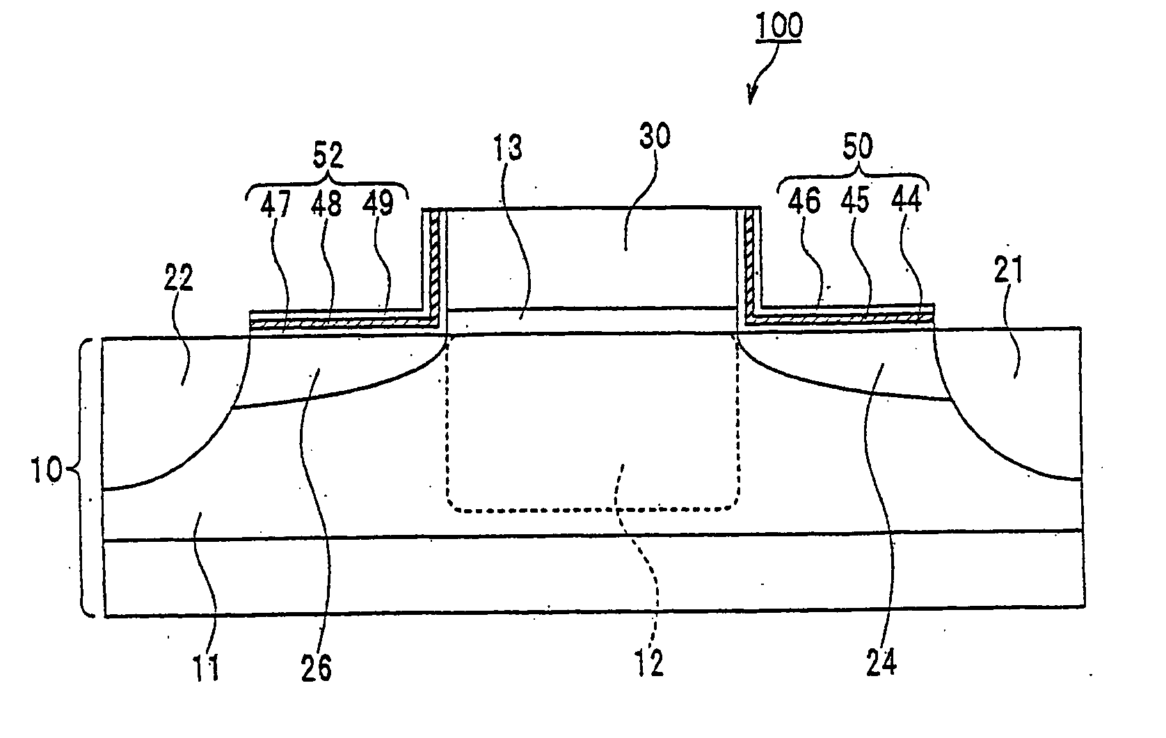
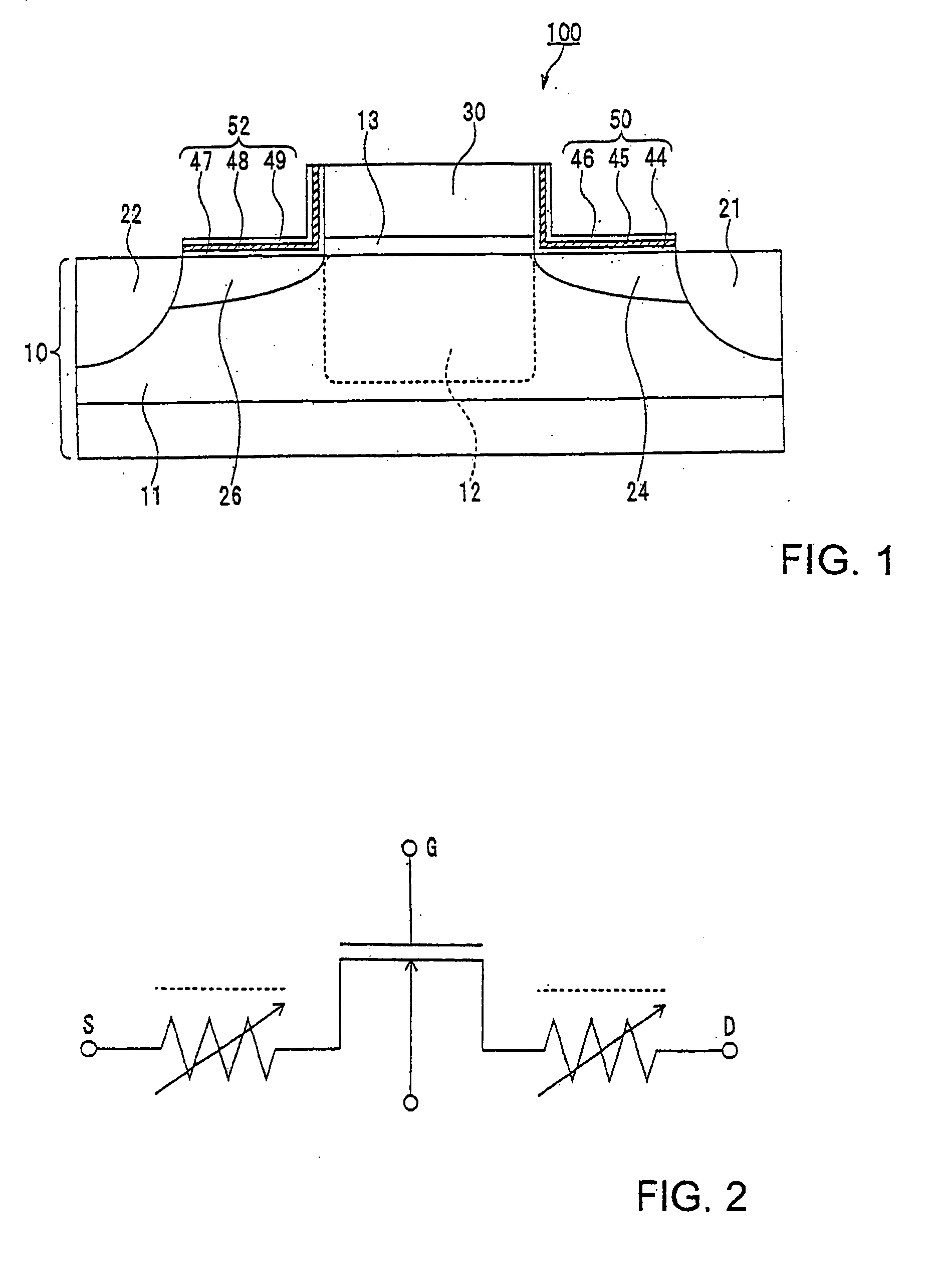
[0023] The structure of a semiconductor nonvolatile memory cell according to the first embodiment of the invention will now be described with reference to FIGS. 1 and 2.
[0024] In FIG. 1, the semiconductor nonvolatile memory cell includes a p-type silicon substrate 10, a P well 11 formed on the silicon substrate 10, separate drain and source regions 21 and 22 made of N+ diffusion layers in the P well 11, and a channel forming region 12 between them. A gate insulation layer 13 is formed on the channel forming region 12, and a gate electrode 30 is formed on the gate insulation layer 13.
[0025] The first variable resistance section 24 is provided between the drain region 21 and the channel forming region 12. The first silicon oxide layer 44, a silicon nitride layer 45, and the second silicon oxide layer 46 are provided on the first variable resistance section 24 to form the first charge storage section 50. The second variable resistance section 26 is provided between the source region ...
second embodiment
[0031] A semiconductor nonvolatile memory cell array according to the second embodiment of the invention will now be described with reference to FIGS. 5-8.
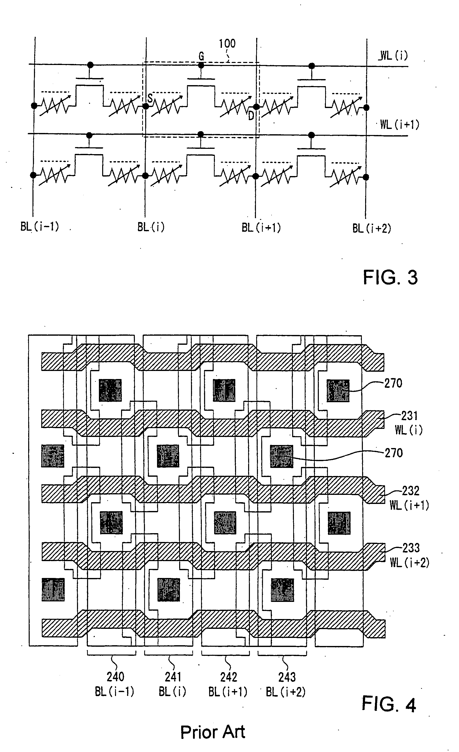
[0032] In FIG. 5, a semiconductor nonvolatile memory cell array has a two dimensional arrangement of semiconductor nonvolatile memory cells (hereinafter “memory cells”). The memory array has a plurality of bit lines, such as BL(i−1) 340, BL(i) 341, BL(i+1) 342, and BL(i+2) 343, arranged in columns and a plurality of word lines, such as WL(i) 331, WL(i+1) 332, and WL(i+2) 333, arranged in rows.
[0033] A plurality of memory cells 351, 352, 353, and 354 are made so as to be connected to one word line and adjacent two bit lines. For example, the memory cell 351 is made so as to be connected to the word line WL(i) 331 and the bit lines BL(i) 341 and BL(i+1) 342, the memory cell 352 to the word line WL(i) 331 and the bit lines BL(i+1) 342 and BL(i+2) 343, the memory cell 353 to the word line WL(i+1) 332 and the bit lines BL(i) 341 and ...
third embodiment
[0053] The memory cell array according to the third embodiment will be described with reference to FIGS. 11(A) and (B). It is different from the memory cell array according to the first embodiment in FIG. 7 in that the first and second salicide regions 60 and 61 are formed on the surface areas of the drain and source regions 21 and 22. The salicide regions 60 and 61 on the drain and source regions 21 and 22 used as bit lines reduce the bit line resistance, stabilizing the operation of the non-volatile memory cell array.
[0054] In FIG. 11(A), the process up to the manufacture of the drain and source regions 21 and 22 is the same as that of the second embodiment described with reference to FIG. 9(A) through FIG. 10(A) and its description will be omitted. After the drain and source regions 21 and 22 are formed in FIG. 10(A), the first and second salicide regions 60 and 61 of cobalt (Co) or titanium (Ti) are formed. Where the ONO laminated body 40 extends over the drain and source regio...
PUM
 Abstract
Description
Claims
Application Information