Hybrid solar cells with thermal deposited semiconductive oxide layer

a solar cell and semi-conductive technology, applied in the field of hybrid solar cells with thermally deposited semi-conductive oxide layers, can solve the problems of reduced long-term stability, difficult production, and high construction cost of devices, and achieve the effect of sufficiently efficient and cheap production

Inactive Publication Date: 2006-01-12
SONY DEUT GMBH
View PDF11 Cites 23 Cited by
  • Summary
  • Abstract
  • Description
  • Claims
  • Application Information

AI Technical Summary

Benefits of technology

[0012] It is therefore an object of the present invention to provide a solar cell which is both

Problems solved by technology

However, such devices have proven to be very expensive to construct, due to the melt and other processing techniques necessary to fabricate the semiconductor layer.
Nevertheless, as pointed out by the authors themselves, the liquid cells described in these publications are difficult to produce and have a reduced long-term stability, wh

Method used


Image

  • Hybrid solar cells with thermal deposited semiconductive oxide layer
  • Hybrid solar cells with thermal deposited semiconductive oxide layer
  • Hybrid solar cells with thermal deposited semiconductive oxide layer

Examples


example 1

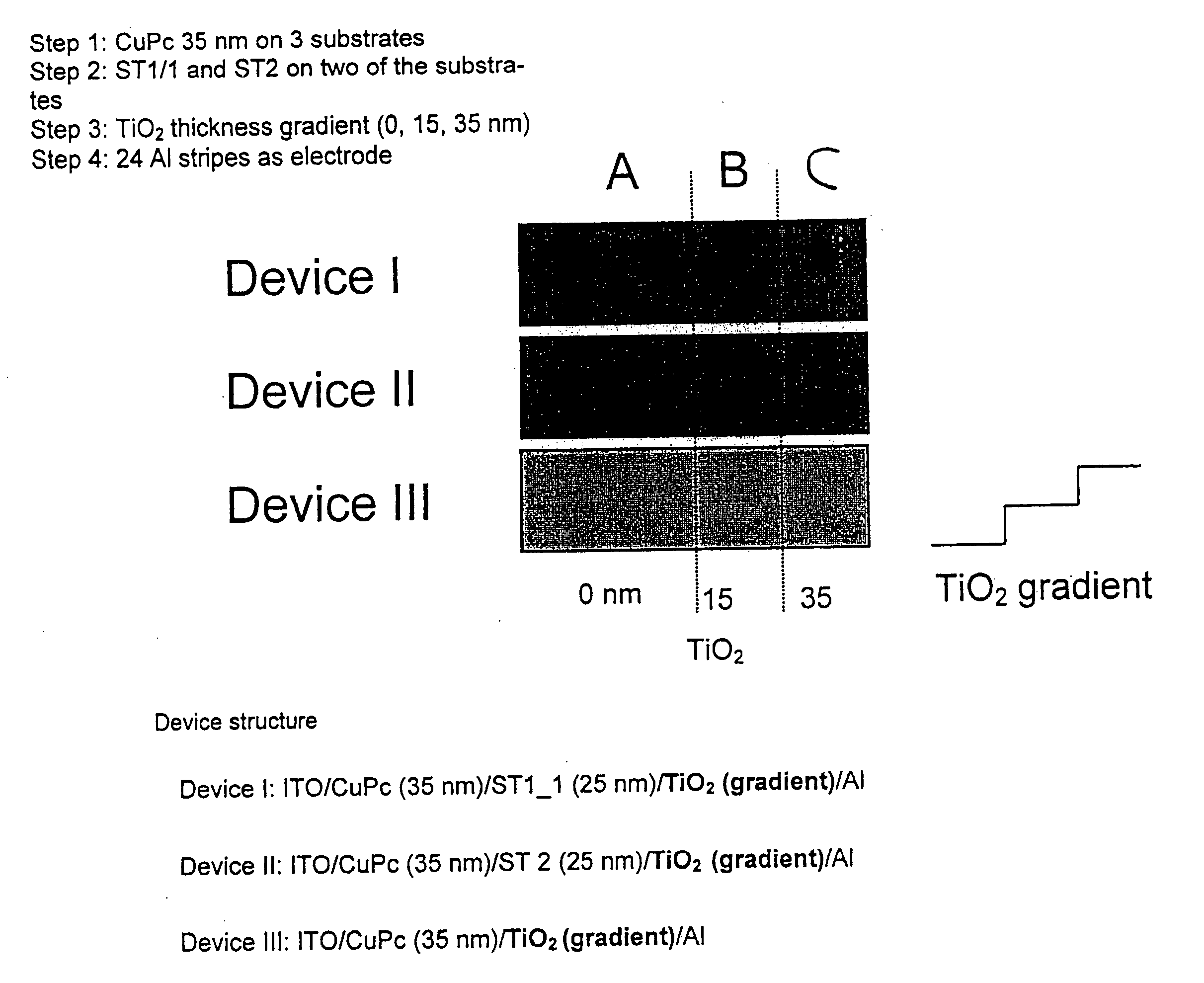
Preparation of a Cell According to the Invention

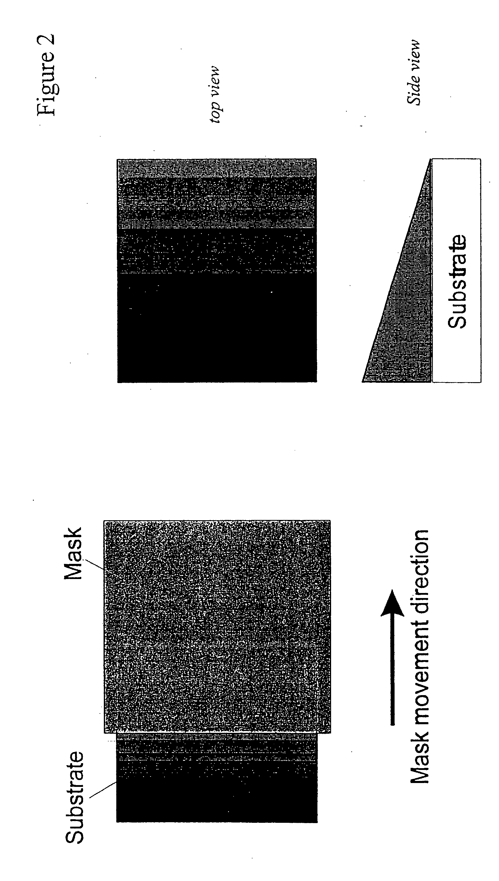
[0054] In a first step according to FIG. 3, commercially available EM coated glass (1) is used as starting material. Suited EM materials are all materials, which can be used to create transparent electrodes, like indium tin oxide, fluorine doped tin oxide, zinc oxide or doped zinc oxide. Further, an evaporated metal electrode (EM layer) selected from metals, like Au, Al, Ca or Mg, or combinations of metals like Al / Li, Mg / Ag, and the like can be used. In order to allow a proper function of the solar cell according to the invention, at least one of the EM-layers should be a TCO.

[0055] The starting material is then coated with a constant thickness layer of HTM (2), which can be applied by vapor deposition, resulting in a HTM-coated device substrate / TCO / HTM (3). Suitable HTM materials can be selected from the group of phthalocyanine and derivatives thereof (with or without a central atom or group of atoms), metal-free and metal containin...

example 2

Characteristics of a Cell Prepared According to the Invention

[0070] The hybrid organic solar cell produced according to example 1 was tested for its current-voltage characteristics and light intensity dependence of Isc and Voc. An Oriel 75W xenon short arc lamp with a water filter, a 345 nm sharp edge filter, a mirror and a PP diffuser was used as the light source. Current-voltage characteristics were measured with an SMU Keithley 2400, an IEEE-card together with a self-developed Labview measuring program (I [A], V [V], Idens [mA / cm2], FF [%], Pmax [mW / cm2], η [%]. Standard measurement parameters were: ambient conditions, 60 mW / cm2 to 100 mW / cm2, a cycle of 0 V to −0.1 V to +1.0 V (illuminated and dark), a 5 mA step size and 3 seconds delay time. The results of the measurements are graphically depicted in FIGS. 5 and 6 and listed in Tables 1 and 2, below.

TABLE 1Current-voltage characteristicsDeviceIsc [mA / cm2]Voc [mV]FF [%]η [%]A (0 nm TiO2)1.86142057.60.75B (15 nm TiO2)2.8164404...


PUM


Abstract

A hybrid solar cell device comprising: a substrate material (substrate), an electrode material (EM), a hole transport material (HTM), a dye material (dye), and a semiconductive oxide layer (SOL), wherein a structure of the hybrid solar cell device is selected from a group consisting of:
Substrate+EM/HTM/dye/SOL/EM, or
Substrate+EM/SOL/dye/HTM/EM, or
Substrate+EM/HTM/SOL/EM, and
wherein the EM is selected from a group consisting of a transparent conductive oxide (TCO), a transparent conductive polymer or a transparent organic material, and a metal, with at least one of the EM layer(s) of the hybrid solar cell being a TCO, and wherein the SOL comprises a dense semiconductive oxide layer.

Description

[0001] This application is a continuation-in-part of application Ser. No. 10 / 799,257, filed Mar. 12, 2004, now pending, which application is a continuation of application Ser. No. 09 / 989,848, filed Nov. 21, 2001, now issued U.S. Pat. No. 6,706,962, both applications being incorporated herein by reference.DESCRIPTION [0002] The present invention is related to the manufacture of organic hybrid solar cells in which the semiconductive oxide layer of the organic hybrid cell is vapor deposited. [0003] Among chief materials used in the past for solar cells have been inorganic semiconductors made from, for example, silicon. However, such devices have proven to be very expensive to construct, due to the melt and other processing techniques necessary to fabricate the semiconductor layer. [0004] In an effort to reduce the cost of solar cells, organic photoconductors and semiconductors have been considered, due to their inexpensive formation by, e.g. thermal evaporation, spin coating, self-asse...

Claims


Application Information

Patent Timeline
IPC IPC(8): B05D5/06
CPCH01G9/2031H01L51/001H01L51/0053Y02E10/549H01L51/4226H01L2251/308Y02E10/542H01L51/0078H10K71/164H10K85/621H10K85/311H10K30/151H10K2102/103H10K30/50
Inventor NELLES, GABRIELLEYASUDA, AKIOSCHMIDT, HANS-WERNERTHELAKKAT, MUKUNDANSCHMITZ, CHRISTOPH
Owner SONY DEUT GMBH
Why Eureka
Try Eureka