Light extraction from a semiconductor light emitting device via chip shaping

a light-emitting device and semiconductor technology, applied in semiconductor devices, basic electric elements, electrical equipment, etc., can solve the problems of low internal quantum efficiency emission layer, low light extraction efficiency, and many optical loss mechanisms in commercial leds, and achieve low loss optical extraction, high injection efficiency, and increased total light extraction

Inactive Publication Date: 2006-01-19
PHILIPS LUMILEDS LIGHTING CO LLC
View PDF49 Cites 83 Cited by
  • Summary
  • Abstract
  • Description
  • Claims
  • Application Information

AI Technical Summary

Benefits of technology

[0020] In some embodiments, by shaping a semiconductor light-emitting device (LED) such that the side surface(s) that are oriented at an angle(s) offset relative to the direction normal to the plane of the light-emitting layer, the total light extraction is increased. By employing a p-n heterojunction for high injection efficiency, and transparent windows for low-loss optical extraction out both the top and side surfaces, high total external quantum effic

Problems solved by technology

Commercial LEDs are non-ideal devices that contain many optical loss mechanisms, e.g. active layer re-absorption, absorption within internal epitaxial layers, finite ohmic contact reflectivity, free-carrier absorption within doped regions.
In particular, for devices with emission layers of low internal quantum efficiency, the loss mechanisms due to the active layer can limit extracted light to only those photons which escape the device without making a second pass through the active layer after emission.
The problem is exacerbated by other loss mechanisms and by the fact that a majority of photon trajectories traverse more than just the vertical thickness of the active layer.
However, fundamental limitations in the materials growth and device physics (e.g. carrier confinement, interfacial recombination) limit the minimum thickness of the active layer at which reasonable radiative efficiencies can be achieved.
Indeed, even in structures of relatively high internal quantum efficiency, loss due to ohmic contacts and free-carrier absorption still compel designs for more first-pass light extraction.
Also, this device does not employ a heterojunction and would suffer reduced injection efficiency at room temperature relative to the published data at T=77 K. Furthermore, the upper extraction window for this homojunction device is not transparent to a substantial portion of the photons generated within the p-n junction active region.
With the internal quantum efficiency of GaAs LEDs typically close to 100% (especially at T=77 K), the relatively lo

Method used


Image

  • Light extraction from a semiconductor light emitting device via chip shaping
  • Light extraction from a semiconductor light emitting device via chip shaping
  • Light extraction from a semiconductor light emitting device via chip shaping

Examples


Embodiment Construction

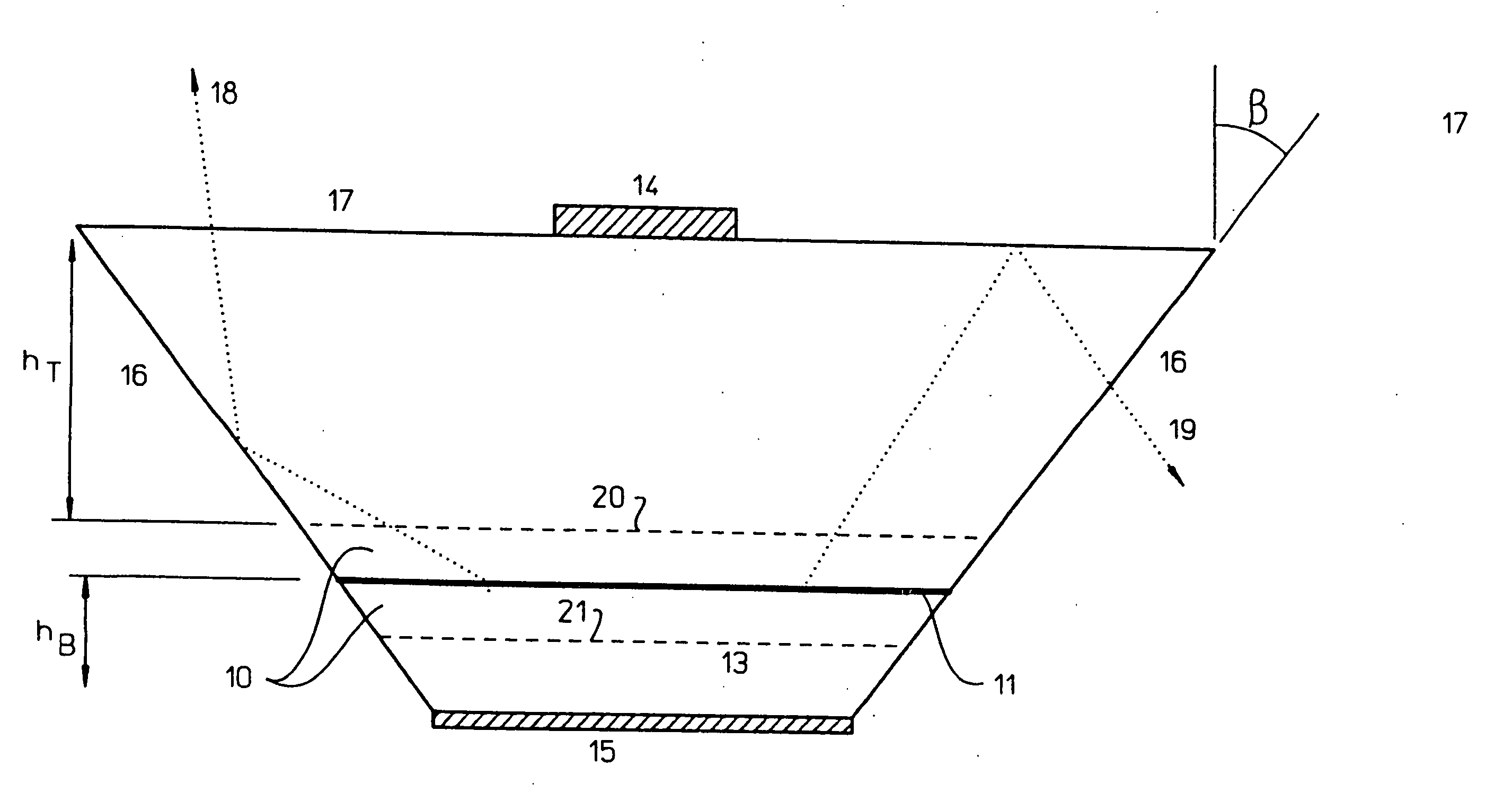
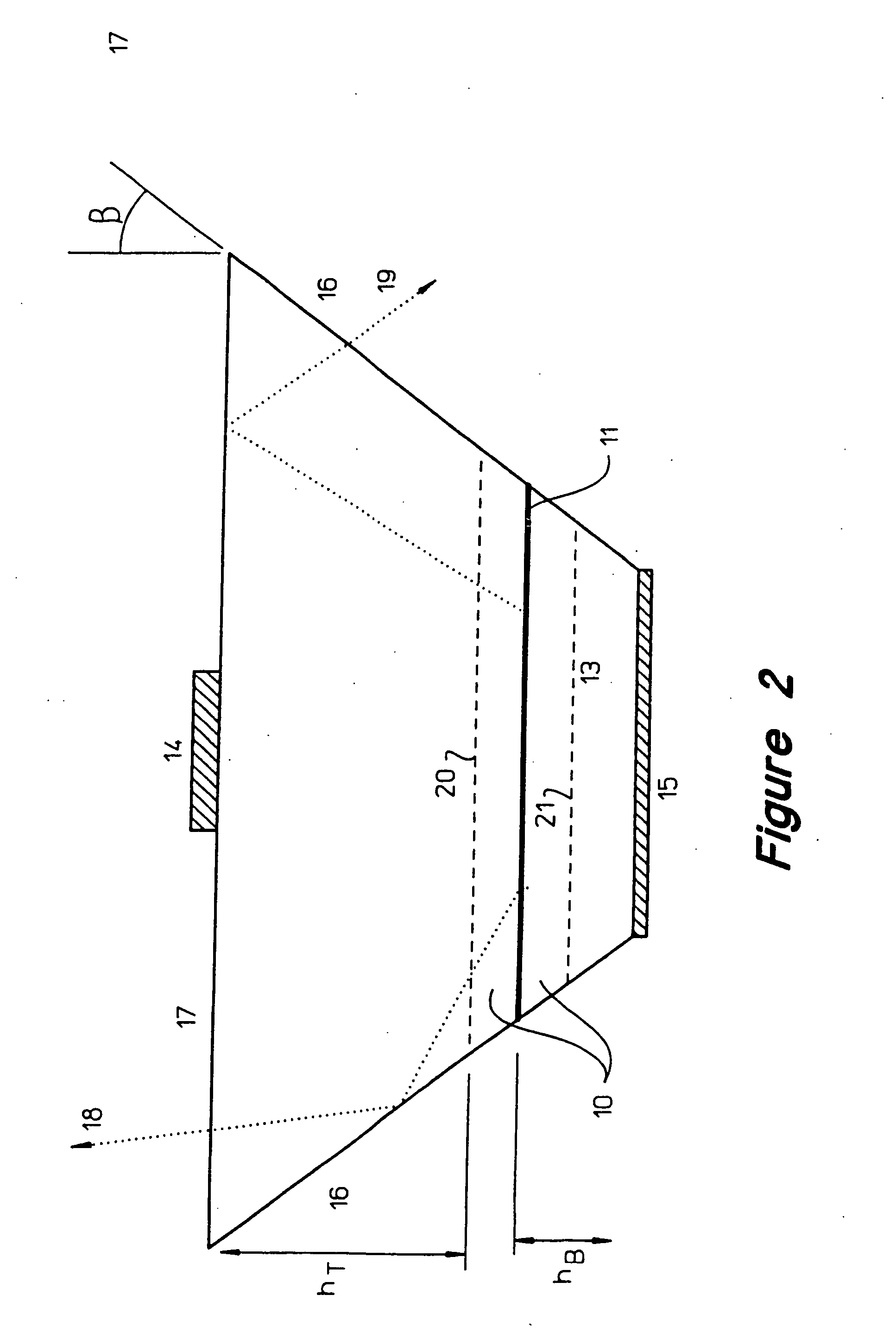
[0047] A side-view of a preferred embodiment of a semiconductor light-emitting device (LED) is shown in FIG. 2. The LED includes a heterostructure comprising a plurality of p- and n-type doped epitaxial layers 10 grown on a substrate, e.g. GaAs, GaP, or sapphire. The p- and n-type layers are arranged to provide a p-n junction region in or near an active region 11. The resulting heterojunction provides for high injection efficiency at room temperature and is essential for devices in high-power applications. The area extent of the p-n junction region defines the active device area. For high-flux applications, the active device area is preferably greater than 150 mil2.

[0048] The growth substrate may optionally be removed and replaced via wafer-bonding, e.g. Kish in U.S. Pat. No. 5,376,580, issued Dec. 27, 1994, or regrown to provide a new substrate with favored characteristics. This is desirable when the growth substrate absorbs the wavelength of light emitted from the active region. ...


PUM


Abstract

A method for designing semiconductor light emitting devices is disclosed wherein the side surfaces (surfaces not parallel to the epitaxial layers) are formed at preferred angles relative to vertical (normal to the plane of the light-emitting active layer) to improve light extraction efficiency and increase total light output efficiency. Device designs are chosen to improve efficiency without resorting to excessive active area-yield loss due to shaping. As such, these designs are suitable for low-cost, high-volume manufacturing of semiconductor light-emitting devices with improved characteristics.

Description

CROSS REFERENCE TO RELATED APPLICATIONS [0001] This is a continuation of U.S. patent application Ser. No. 10 / 867,936 filed on Jun. 14, 2004, now U.S. Pat. No. 6,946,309, which is a divisional of U.S. patent application Ser. No. 10 / 095,552 filed on Mar. 11, 2002, now U.S. Pat. No. 6,784,463, which is a continuation in part of U.S. patent application Ser. No. 09 / 732,326 filed on Dec. 6, 2000, now U.S. Pat. No. 6,570,190, which is a continuation of U.S. patent application Ser. No. 08 / 868,009 filed on Jun. 3, 1997, now U.S. Pat. No. 6,229,160. U.S. Pat. Nos. 6,229,160, 6,570,190, 6,784,463, and 6,946,309 are incorporated herein by reference in their entirety.BACKGROUND [0002] 1. Field of Invention [0003] Embodiments of the invention relate to the process of designing and fabricating semiconductor light-emitting devices. In particular, embodiments of the invention are directed towards improving the light extraction efficiency and increasing the total light output of these devices. [0004]...

Claims


Application Information

Patent Timeline
IPC IPC(8): H01L33/00H01L33/02H01L33/08H01L33/14H01L33/20
CPCH01L33/02H01L33/08H01L2224/13H01L33/20H01L33/14H01L24/03H01L24/05H01L24/06H01L2224/05568H01L2224/05573H01L2224/06102H01L2224/0615H01L2224/1703H01L2224/05611H01L2924/00014H01L2224/05624H01L2224/05639H01L2224/05644H01L2224/05655H01L2224/05664H01L2224/05666H01L2224/05669H01L2224/05671H01L2224/05684
Inventor KRAMES, MICHAEL R.KISH, FRED A. JR.TAN, TUN S.
Owner PHILIPS LUMILEDS LIGHTING CO LLC
Why Eureka
Try Eureka