

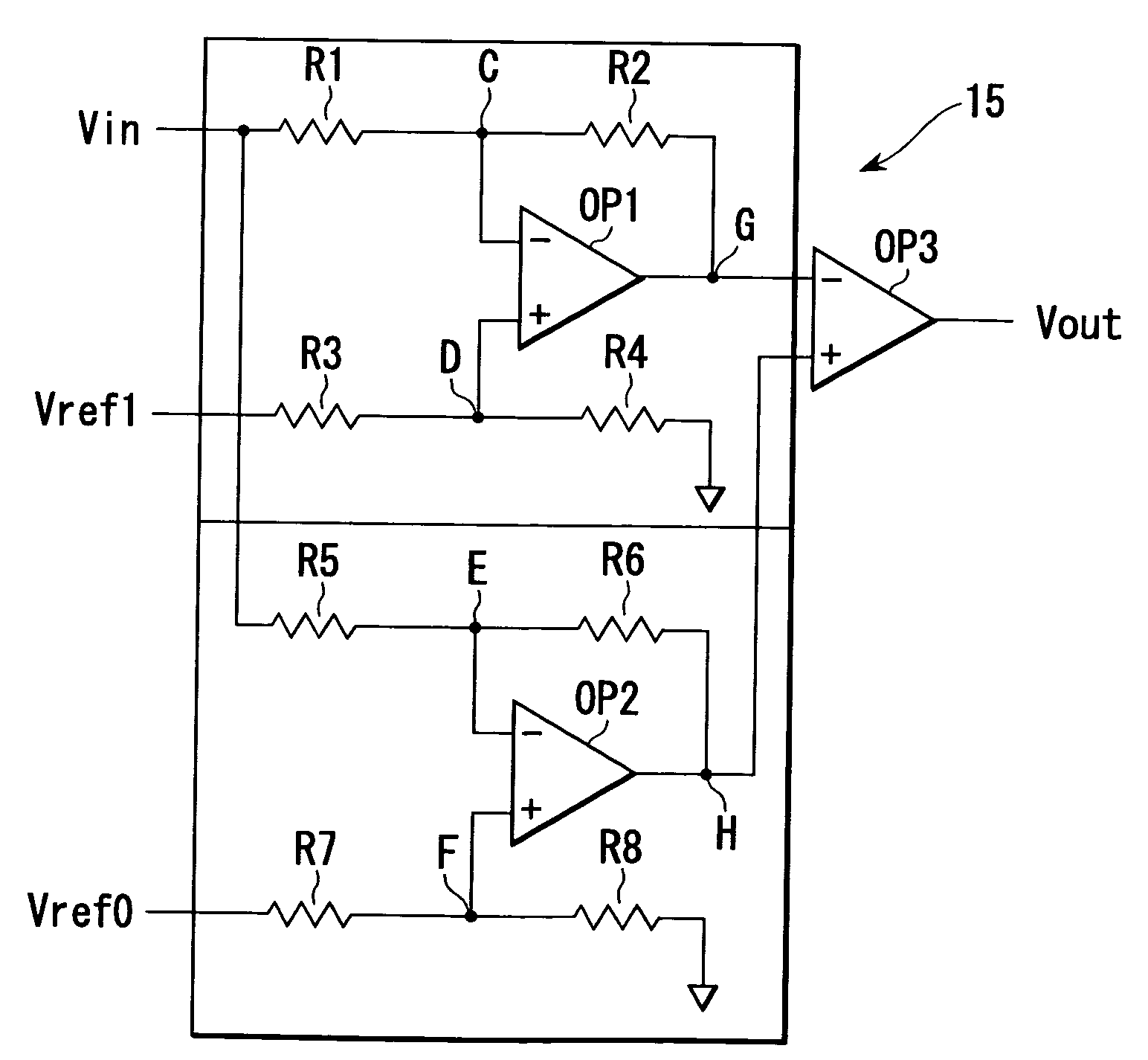
Semiconductor apparatus having logic level decision circuit and inter-semiconductor apparatus signal transmission system
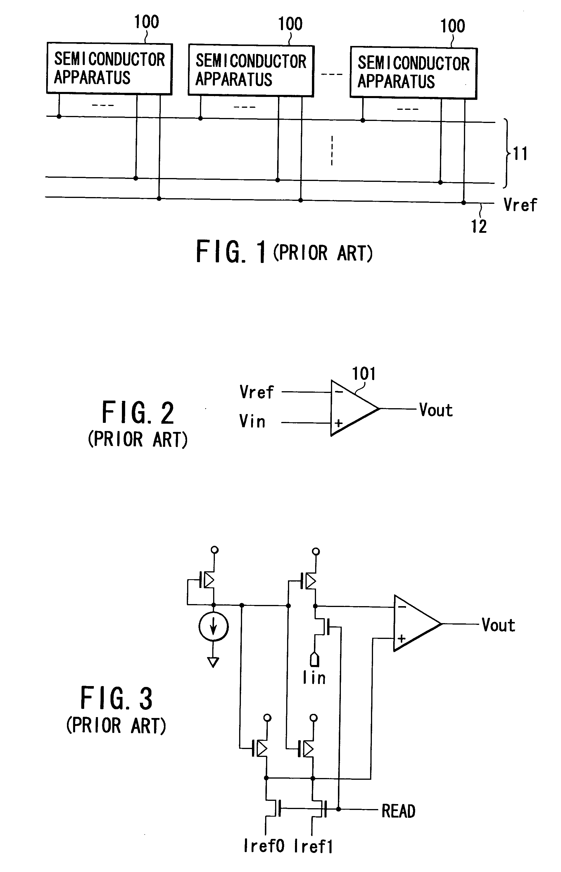
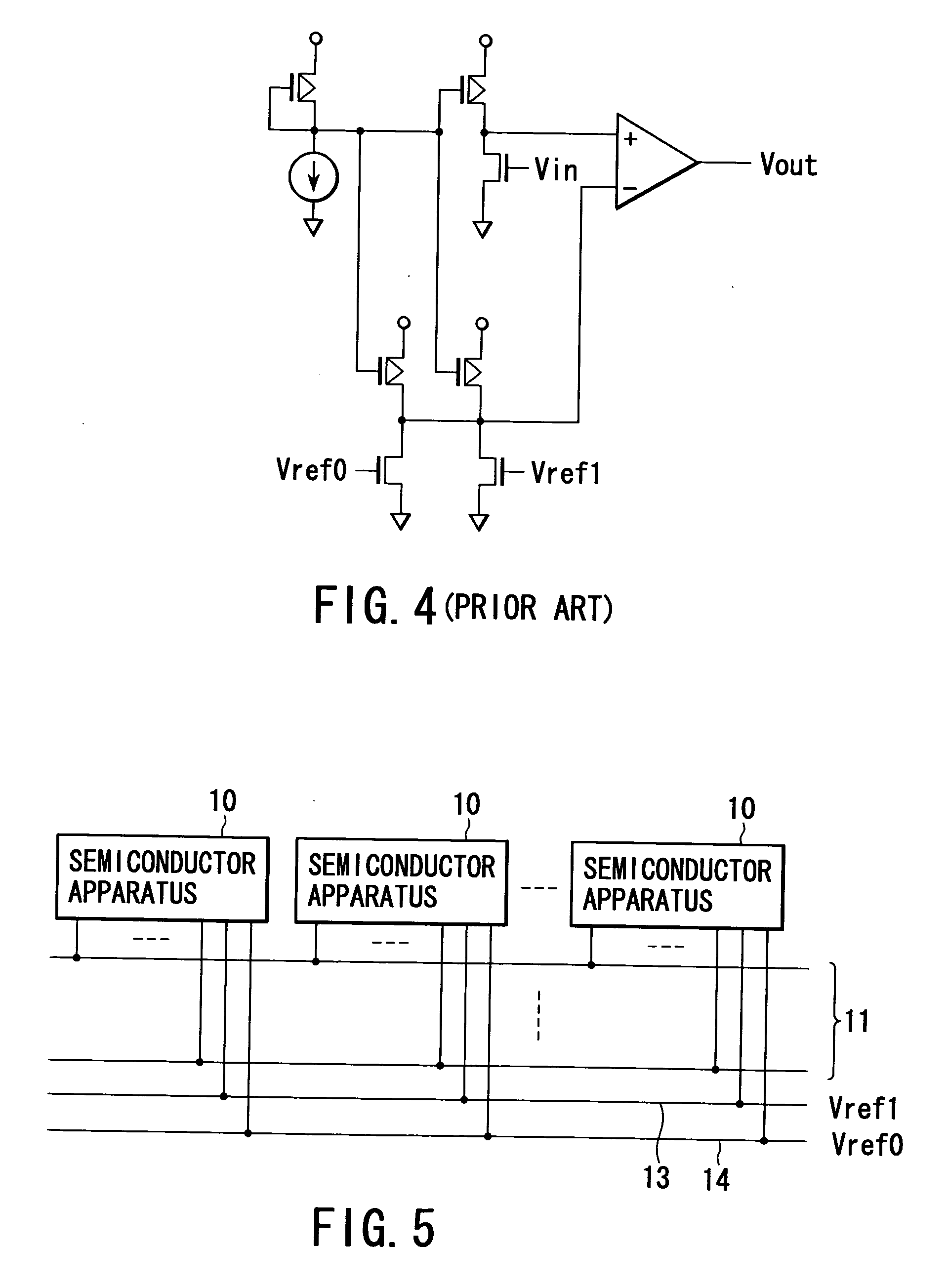
a technology of logic level decision and logic level, which is applied in the direction of logic circuits using specific components, pulse techniques, instruments, etc., can solve the problems of low supply voltage, easy malfunction of input receivers, and easy occurrence of malfunctions
- Summary
- Abstract
- Description
- Claims
- Application Information
AI Technical Summary
Benefits of technology
Problems solved by technology
Method used
Image

Examples
example 1
APPLICABLE EXAMPLE 1
[0153] As one of applicable examples of the MRAM, FIG. 21 shows a digital subscriber line (DSL) data path portion of a digital subscriber line (DSL) modem. This modem includes a programmable digital signal processor (DSP) 151, an analog-to-digital converter (A / D) and digital-to-analog converter (D / A) 152, a transmission driver 153, and a receiver amplifier 154. In FIG. 21, the band pass filter is omitted, and an MRAM 155 and an EEPROM 156 are shown instead as an optional memory of various types capable of holding a line code program.
[0154] In this example, as the memory for holding the line code program, two memories MRAM and EEPROM are used, but the EEPROM may be replaced by the MRAM, that is, without using two memories, only the MRAM may be used.
example 2
APPLICABLE EXAMPLE 2
[0155] As another applicable example of the MRAM, FIG. 22 shows a portion for realizing communication function in a cellphone terminal 300. As shown in FIG. 22, the portion for realizing the communication function comprises a transmission and reception antenna 201, an antenna duplexer 202, a receiver 203, a base band processor 204, a digital signal processor (DSP) 205 used as audio codec, a loudspeaker 206, a microphone 207, a transmitter 208, and a frequency synthesizer 209.
[0156] Also as shown in FIG. 22, the cellphone terminal 300 has a controller 200 for controlling the parts of the cellphone terminal. The controller 200 is a microcomputer composed by connecting a CPU 221, a ROM 222, an MRAM 223, and a flash memory 224 by way of a CPU bus 225.
[0157] Herein, the ROM 222 preliminarily stores programs to be executed in the CPU 221, and necessary data such as display font. The MRAM 223 is mainly used as a working region, and specifically it is used when storing...
example 3
APPLICABLE EXAMPLE 3
[0160] FIGS. 23 to 27 show an example in which the MRAM is applied in a card holding media contents such as smart media (MRAM card).
[0161] In a top view in FIG. 23, reference numeral 400 is an MRAM card main body, 401 is an MRAM chip, 402 is an opening, 403 is a shutter, and 404 denotes plural external terminals. The MRAM chip 401 is contained in the MRAM card main body 400, and is exposed to outside through the opening 402. While carrying the MRAM card, the MRAM chip 401 is covered with the shutter 403. The shutter 403 is made of a material having an effect of shielding an external magnetic field, such as ceramic material. When transferring the data, the shutter 403 is released, and the MRAM chip 401 is exposed. The external terminals 404 are for taking out the contents data stored in the MRAM card to outside.
[0162]FIGS. 24 and 25 are a top view and a side view of a transfer device of card insert type for transferring data on the MRAM card. A second MRAM card ...
PUM
 Abstract
Description
Claims
Application Information