

Method and apparatus of forming thin film using atomic layer deposition
a technology of atomic layer and forming method, which is applied in the direction of chemical vapor deposition coating, coating, coating process, etc., can solve the problems of difficult selective control of step coverage in a specific portion, unfavorable thermal effects of semiconductor devices, and the typical cvd method used to form thin films that do not generally provide excellent step coverage, etc., to improve the reaction rate of ald process, improve the growth rate of tin thin films, and improve the effect of
- Summary
- Abstract
- Description
- Claims
- Application Information
AI Technical Summary
Benefits of technology
Problems solved by technology
Method used
Image

Examples
embodiment 1
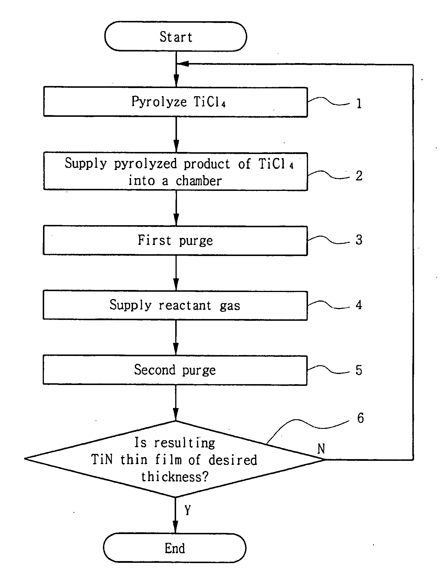
[0027]FIG. 1 is a flow chart illustrating a method for forming a TiN thin film according to a first embodiment of the present invention.
[0028] In the method for forming a TiN thin film according to a first embodiment of the present invention, titanium chloride (TiCl4) is thermally pyrolyzed into TiCl3 or TiCl2, and an atomic layer deposition (ALD) process is performed using the TiCl3 or TiCl2 as a source gas.
[0029] As shown in FIG. 1, the formation of the TiN thin film may be performed as follows.
[0030] In a first step 1, titanium chloride (TiCl4) as a source gas is heated using a heater, and is made to be thermally pyrolyzed into TiCl3 or TiCl2. In a preferred embodiment, the titanium chloride (TiCl4) must be heated at a temperature of about 350° C. or higher to thermally pyrolyze the titanium chloride (TiCl4).
[0031] In a second step 2, the pyrolyzed product, TiCl3 or TiCl2 is introduced into a chamber having a substrate on which a TiN thin film will be formed.
[0032] In a thir...
embodiment 2
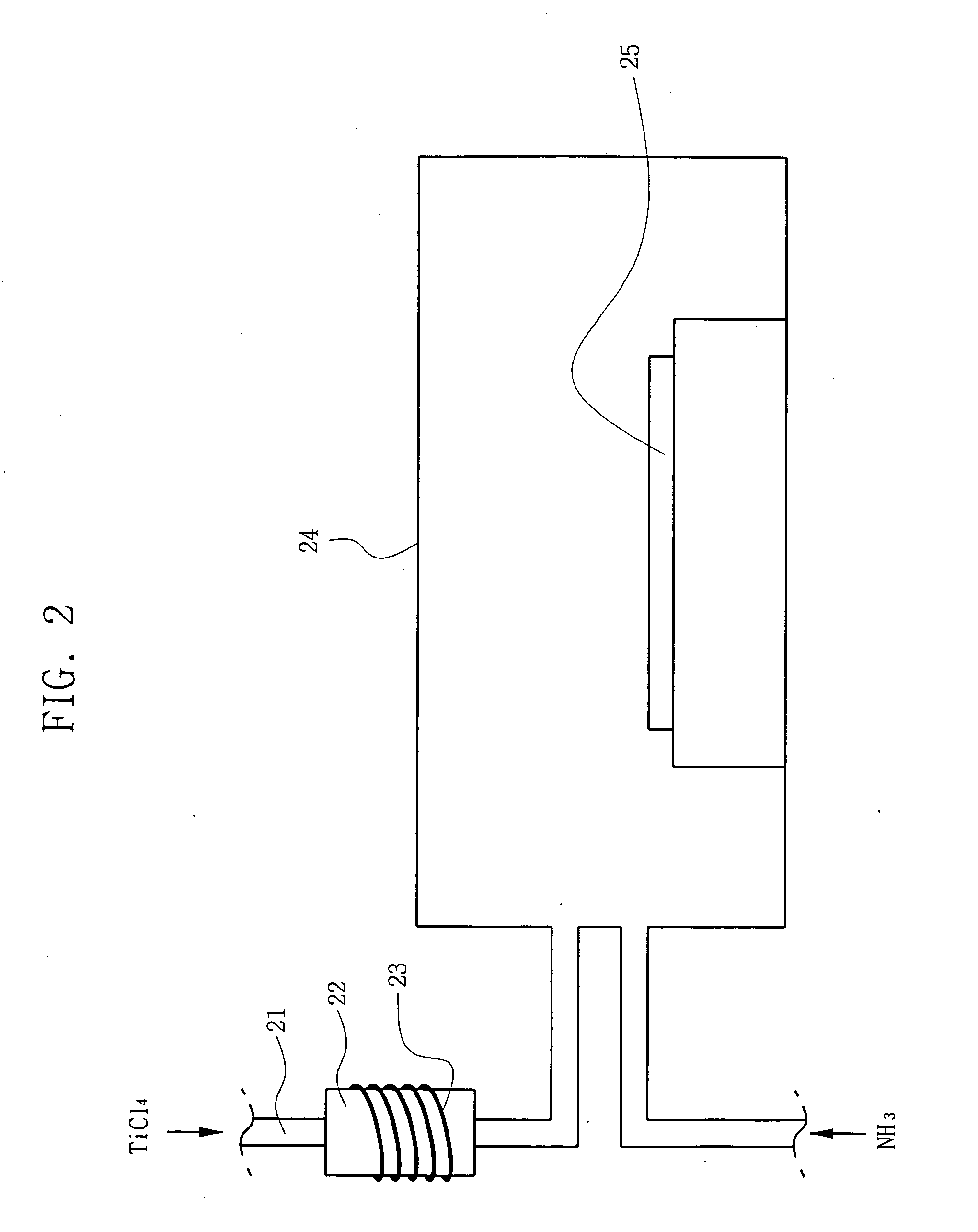
[0038]FIG. 3 is a flow chart illustrating a method of forming a TiN thin film according to a second embodiment of the present invention.
[0039] In the method of forming a TiN thin film according to a second embodiment of the present invention, titanium chloride (TiCl4) is pyrolyzed using heat and hydrogen (H2) gas into TiCl3 or TiCl2, and an atomic layer deposition (ALD) process is performed using the TiCl3 or TiCl2 as a source gas.
[0040] As shown in FIG. 3, the formation of the TiN thin film may be performed as follows.
[0041] In a first step 31, titanium chloride (TiCl4) as a source gas and hydrogen (H2) gas as a decomposition accelerant gas are heated using a heater. The reason to heat the H2 and the TiCl4 together is to activate the H2 so as to maximize the decomposition effect of the TiCl4. The titanium chloride (TiCl4) must be heated at a temperature of 350° C. or higher to pyrolyze the titanium chloride (TiCl4).
[0042] In a second step 32, the heated gas by the heater in the...
embodiment 3
[0050] In another embodiment of the present invention, TiCl4 is first introduced into a chamber holding the substrate on which the thin film is to be formed. H2 is then heated by a heater and introduced into the chamber to activate and thereby decompose the TiCl4. The pre-heating of the H2 is to maximize the decomposition of TiCl4. As such, the pyrolyzed product of such a process—TiCl3 or TiCl2—is adsorbed on the substrate. Then, NH3 is introduced as a reactant gas into the chamber, so as to react with the TiCl3 or TiCl2 adsorbed on the substrate, thereby forming a TiN thin film.
[0051] As described above, according to the embodiments of the present invention, the method of forming the TiN thin film and the apparatus thereof can provide an improved growth rate of the TiN thin film while using a low temperature process in an ALD process.
[0052] Furthermore, the method of forming the TiN thin film and the apparatus thereof according to the present invention improve the throughput per ...
PUM
| Property | Measurement | Unit |
|---|---|---|
| temperature | aaaaa | aaaaa |
| aspect ratio | aaaaa | aaaaa |
| transparent | aaaaa | aaaaa |
Abstract
Description
Claims
Application Information