Sputter deposition and etching of metallization seed layer for overhang and sidewall improvement

a seed layer and metallization technology, applied in the field of sputter etching process, can solve the problems of increasing the difficulty of sputtering technology, reducing the feature size of advanced integrated circuits, and the same problems, and achieve the effect of high selectivity

a seed layer and metallization technology, applied in the field of sputter etching process, can solve the problems of increasing the difficulty of sputtering technology, reducing the feature size of advanced integrated circuits, and the same problems, and achieve the effect of high selectivity

US20060030151A1Active Publication Date: 2006-02-09APPLIED MATERIALS INC

Image

  • Sputter deposition and etching of metallization seed layer for overhang and sidewall improvement
  • Sputter deposition and etching of metallization seed layer for overhang and sidewall improvement
  • Sputter deposition and etching of metallization seed layer for overhang and sidewall improvement

Examples


Embodiment Construction

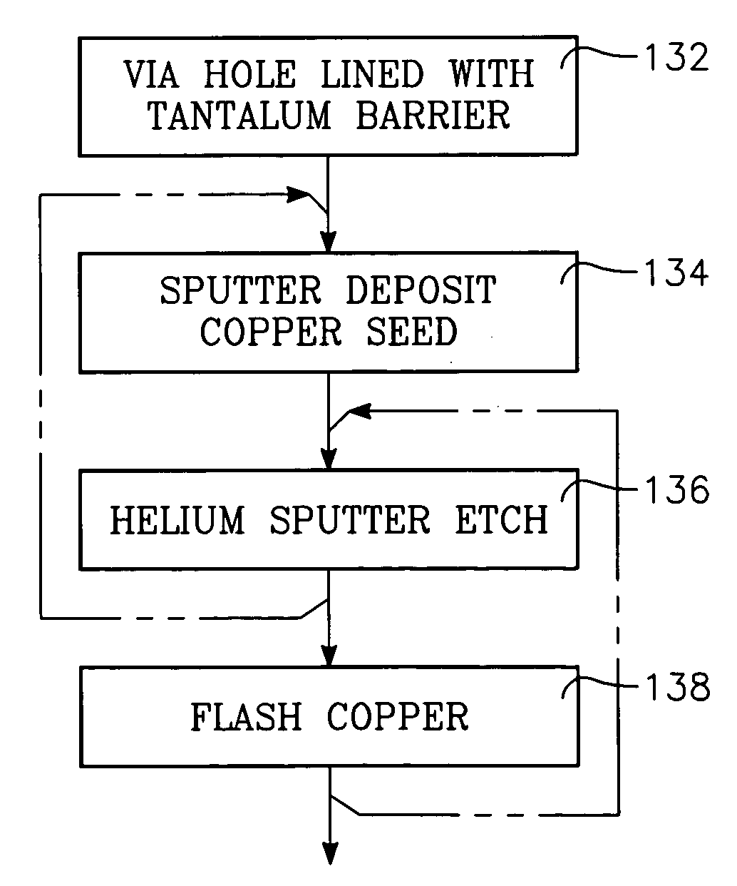
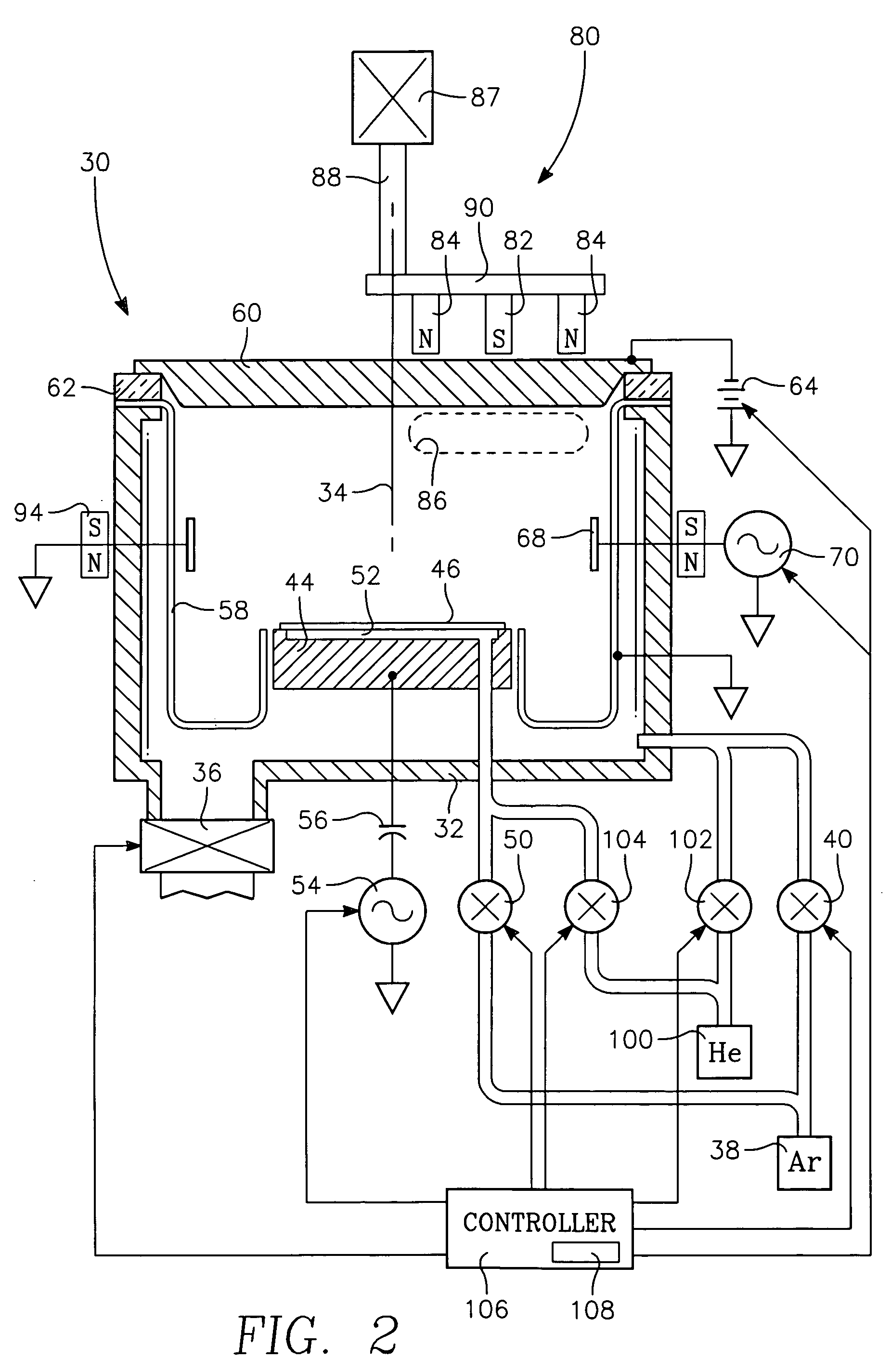
[0024] One embodiment of the invention may be practiced in a sputter reactor capable of both sputtering depositing target material on a substrate and sputter etching the same substrate The sputter etching of the overhangs or other features is advantageously performed with a gas lighter than the usual argon sputter working gas. One example of such a magnetron sputter reactor 30 is illustrated in schematic cross sectional view in FIG. 2 is available from Applied Materials, Inc. of Santa Clara, Calif. although it was previously used with a tantalum target for barrier deposition rather than for copper or aluminum sputtering. The reactor 30 includes a vacuum chamber 32 arranged generally symmetrically about a central axis 34. A vacuum pump system 36 pumps the chamber 32 to a very low base pressure in the range of 10−6 Torr. However, an argon gas source 38 connected to the chamber 32 through a mass flow controller 40 supplies argon as a sputter working gas into the chamber 32. The argon p...


PUM

PropertyMeasurementUnit
thicknessaaaaaaaaaa
widthaaaaaaaaaa
widthaaaaaaaaaa

Abstract

An integrated sputtering method and reactor for copper or aluminum seed layers in which a plasma sputter reactor initially deposits a thin conformal layer onto a substrate including a high-aspect ratio hole subject to the formation of overhangs. After the seed deposition, the same sputter reactor is used to sputter etch the substrate with energetic light ions, especially helium, having an energy sufficiently low that it selectively etches the metallization to the heavier underlying barrier layer, for example, copper over tantalum or aluminum over titanium. An RF inductive coil generates the plasma during the sputtering etching while the target power is turned off. A final copper flash step deposits copper over the bare barrier field region before copper is electrochemically plated to fill the hole. The invention also includes a simultaneous sputter deposition and sputter etch, and an energetic ion processing of the copper seed sidewall.

Description

FIELD OF THE INVENTION [0001] The invention relates generally to sputtering of materials. In particular, the invention relates to a sputter etching process performed as part of a sputter deposition process. BACKGROUND ART [0002] Sputtering, alternatively called physical vapor deposition (PVD), is the most prevalent method of depositing layers of metals and related materials in the fabrication of integrated circuits. Although originally sputtering was principally used to deposit substantially planar layers for horizontal interconnects and other electrical structures, more recently various sputtering techniques have been developed to coat thin, substantially conformal metal or metal nitride layers in holes formed in a dielectric layer. Such holes can be very narrow vias penetrating the dielectric layer to provide vertical electrical interconnections between wiring layers or can be relatively narrow trenches formed in the surface of the dielectric layer to provide horizontal electrical...

Claims


Application Information

Patent Timeline
09 Feb 2006
Publication
US20060030151A1
IPC
H01L21/4763
CPC
H01L21/2855; H01L21/76843; H01L2221/1089; H01L21/76873; H01L21/76865
Inventors
DING, PEIJUN; ZHANG, FUHONG