Quantum cascade laser device

a laser device and quantum cascade technology, applied in semiconductor lasers, laser details, electrical devices, etc., can solve the problem that the inversion of the population required for laser oscillation is typically impossible, and achieve the effect of stabilizing the energy distribution of carriers in the region b and stabilizing the energy distribution

Inactive Publication Date: 2006-02-23
CANON KK
View PDF15 Cites 32 Cited by
  • Summary
  • Abstract
  • Description
  • Claims
  • Application Information

AI Technical Summary

Benefits of technology

[0011] Since a tunneling that is allowed by an interaction with light (i.e., photon-assisted tunneling) is used as an optical transition, the binding of two energy levels relating to the optical transition in the region A and the region B becomes selective. According to this structure, a non-radiative current can be reduced, and in addition, the transit time of carriers in the region A can be limited by the potential barrier. As a result, the energy distribution of carriers in the region B can be stabilized as follows. When the relaxation time of carriers in the region B is shorter than the transit time of carriers in the region A, the energy distribution of unstable carriers in the region B, or the carriers remaining in a warmed up state, is cooled so as to approach a quasi-Fermi distribution. With reference to the energy relaxation, the energy relaxation time of carriers in the region B becomes shorter than the transit time of carriers in the region A including the photon-assisted tunneling by utilizing a high-speed relaxation mechanism. As a result, the energy distribution of carriers in the region B can be stabilized. Accordingly, this structure can more reliably provide the population inversion between two energy levels relating to a radiative transition in the region A that is combined with the region B.
[0012] In order to achie

Problems solved by technology

As a result, a population inversion required for

Method used


Image

  • Quantum cascade laser device
  • Quantum cascade laser device
  • Quantum cascade laser device

Examples


Embodiment Construction

[0021] An exemplary embodiment of the present invention will now be described with reference to FIG. 1.

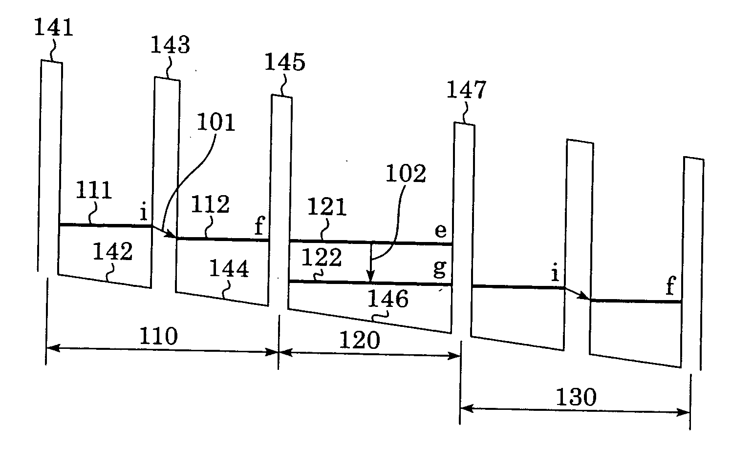
[0022] In a multiple quantum well in a semiconductor device according to the present invention, a region A 110 and a region B 120 are periodically repeated as a repeating unit. FIG. 1 shows a part of the structure of a conduction band when an electric field is applied to the multiple quantum well.

[0023] The region A 110 includes potential barriers 141, 143, and 145, and quantum wells 142 and 144. This structure provides an energy level i (111) and an energy level f (112). The energy level i and the energy level f are spatially separated by the potential barrier 143. However, when the energy levels are designed so that a weak-coupling (i.e. overlap of wave functions is relatively small) is formed, an electron is transported from the energy level i to the energy level f by photon-assisted tunneling 101.

[0024] As shown in FIG. 1, when energy Ei of the energy level i is larger than ...


PUM


Abstract

A device includes a multiple quantum well with potential barriers and quantum wells, and an electric field element for applying an electric field thereto. The multiple quantum well includes at least two regions A and a region B disposed therebetween. The region A includes a plurality of energy levels, and a carrier is transported from a specific energy level i to a specific energy level f in the region A through one of the potential barriers by photon-assisted tunneling. The region B includes a plurality of energy levels, and an energy relaxation is performed with a relaxation time shorter than a transit time of the carrier in the region A from a specific energy level e to a specific energy level g in the region B. When an electric field is applied, electric current flows through the multiple quantum well and light is emitted or absorbed in the region A.

Description

BACKGROUND OF THE INVENTION [0001] 1. Field of the Invention [0002] The present invention relates to a current injection-type optical semiconductor device and a semiconductor laser device in a frequency domain of a millimeter-wave band to a terahertz band (for example, from 30 GHz to 30 THz). [0003] 2. Description of the Related Art [0004] A quantum cascade laser in which carrier transitions are performed between energy levels in the same energy band of either a conduction band or a valence band has been disclosed as a semiconductor laser. Since the oscillation wavelength of such a laser depends on the energy gap between two energy levels relating to optical transition, the oscillation wavelength can be selected over a wide spectrum range (for example, from a mid-infrared region to a terahertz band). In one example, laser light was achieved in a quantum cascade laser in which the oscillation wavelength was selected at 4.2 μm in the mid-infrared region. In another example, as disclos...

Claims


Application Information

Patent Timeline
IPC IPC(8): H01S5/00
CPCB82Y20/00H01S5/22H01S2302/02H01S5/3422H01S5/34313H01S5/3086
Inventor SEKIGUCHI, RYOTAOUCHI, TOSHIHIKO
Owner CANON KK
Why Eureka
Try Eureka