
Multiple GaInNAs quantum wells for high power applications

a quantum well and quantum well technology, applied in the field of multi-purpose devices, can solve the problems of limiting performance, short wavelength of conventional gaas devices (850 nm) and limiting optical power, and achieve the effect of improving power outpu

Inactive Publication Date: 2006-02-23
THE BOARD OF TRUSTEES OF THE LELAND STANFORD JUNIOR UNIV
View PDF17 Cites 14 Cited by
  • Summary
  • Abstract
  • Description
  • Claims
  • Application Information

AI Technical Summary

Benefits of technology

[0013] The present invention is directed to an approach for improving the power output of an optical-electronic semiconductor device operating at wavelengths approaching and longer than 1.3 μm using multiple quantum well layers with strain compensation for t

Problems solved by technology

However, the relatively short wavelength of conventional GaAs devices (e.g., 850 nm) limits performance due to the wavelength dependent dispersion and loss properties of optical fiber.
Additionally, the short wavelength limits the permissible optical power because of eye safety considerations.
Growing GaInAs quantum wells on GaAs with optical wavelengths beyond 1.1 μm is difficult because increasing indium content further leads to the formation of crystalline defects and mechanical tension, compression or shear in and around the active layer.
This internal stress can be attributable to, among other factors, lattice mismatch between the active region and the substrate, and improper temperature control during manufacture of the laser diode device.
Inadequate temperature control during manufacture can also result in a higher threshold current of laser oscillation and poor temperature characteristics.
The addition of more indium to the GaInAs quantum well material, in an attempt to achieve longer wavelengths, is a limited approach because both the strain energy and the quantum confinement energy increase with increasing indium content.
Although GaInNAs-based laser devices can provide emissions up to 1.3 μm it is challenging to achieve both longer wavelength emission approaching and beyond 1.3 μm and high power output.

Method used


Image

  • Multiple GaInNAs quantum wells for high power applications
  • Multiple GaInNAs quantum wells for high power applications
  • Multiple GaInNAs quantum wells for high power applications

Examples


Embodiment Construction

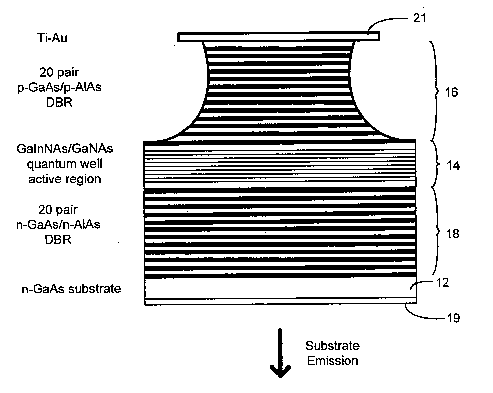
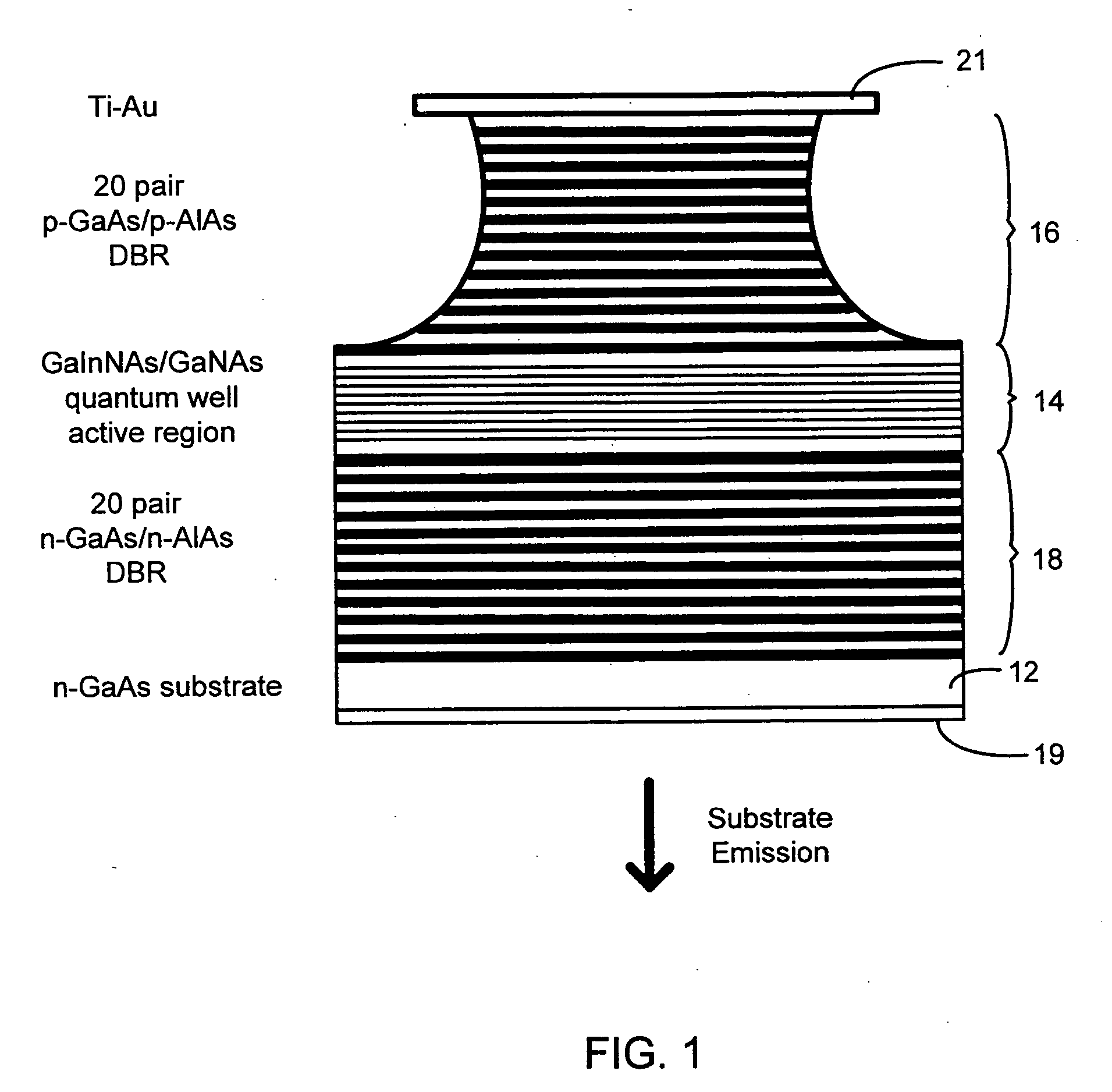
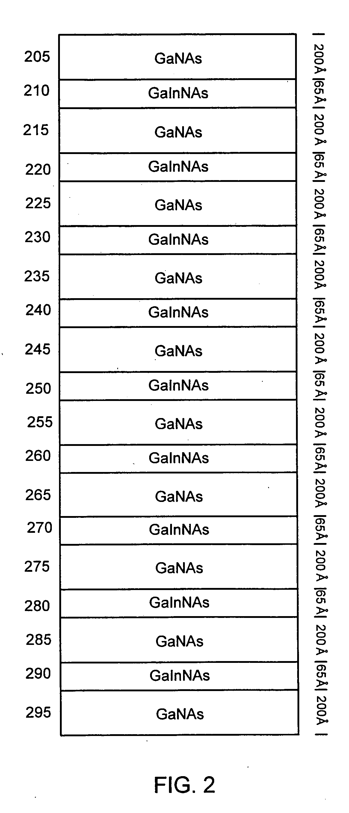
[0030] The present invention is directed to a method and an optical device for achieving higher optical power output with emission at longer wavelengths. According to one aspect of the present invention, it has been discovered that tensile-strained GaNAs-based barrier layers may be used to compensate for compressively strained GaInNAs-based quantum well layers. A strained layer lattice can be grown by alternating layers that are under appropriate compression and tension. By offsetting the compressive strain generated by multiple quantum wells with tensile-strained barrier layers, a greater number of quantum wells may be formed. In this regard, an active region with multiple quantum wells increases the total thickness of the active area beyond the inherent critical thickness of the GaInNAs material.

[0031] The present invention is believed to be applicable to a wide variety of circuit arrangements including optical semiconductor devices and, more specifically, to such circuit arrange...


PUM


Abstract

In connection with an optical-electronic semiconductor device, improved photoluminescent output is provided at wavelengths approaching and beyond 1.3 μm. According to one aspect, a multiple quantum well strain compensated structure is formed using a GaInNAs-based quantum well laser diode with GaNAs-based barrier layers. By growing tensile-strained GaNAs barrier layers, a larger active region with multiple quantum wells can be formed increasing the optical gain of the device. In example implementations, both edge emitting laser devices and vertical cavity surface emitting laser (VCSEL) devices can be grown with at least several quantum wells, for example, nine quantum wells, and with room temperature emission approaching and beyond 1.3 μm.

Description

RELATED PATENT DOCUMENTS [0001] This is a continuation of U.S. patent application Ser. No. 10 / 223,404, filed on Aug. 19, 2002 (STFD.028PA) and bearing the same title, and which is a continuation-in-part of U.S. patent applications Ser. No. 09 / 738,534, filed on Dec. 15, 2000 (STFD.012PA) and entitled “LASER DIODE DEVICE WITH NITROGEN INCORPORATING BARRIER,” and Ser. No. 09 / 738,907, filed on Dec. 15, 2000 (STFD.101PA) and entitled “METHOD FOR MANUFACTURING LASER DIODE WITH NITROGEN INCORPORATING BARRIER.” Each of these patent documents is fully incorporated herein by reference priority to which is claimed under 35 U.S.C. § 120 for common subject matter. BACKGROUND STATEMENTS [0002] The inventive aspects disclosed herein were made with Government support under contract N00014-01-100010 awarded by the Office of Naval Research. The Government has certain rights in these inventive aspects.FEDERALLY-SPONSORED RESEARCH AND DEVELOPMENT [0003] This invention was made with Government Support u...

Claims


Application Information

Patent Timeline
IPC IPC(8): H01S5/00H01S5/20H01L21/00H01S5/183H01S5/32H01S5/323
CPCB82Y20/00H01S5/18305H01S5/3201H01S2302/00H01S5/32366H01S5/34306H01S5/3211
Inventor HA, WONILLGAMBIN, VINCENTHARRIS, JAMES S.
Owner THE BOARD OF TRUSTEES OF THE LELAND STANFORD JUNIOR UNIV
Learn More