Supercharge Your Innovation With Domain-Expert AI Agents!

Event-driven logic circuit

a logic circuit and event-driven technology, applied in the field of logic circuits, can solve the problems of high activation yield, complex clock tree structure, high activation yield, etc., and achieve the effects of low power consumption, reduced input load and activation yield, and high speed operation

Inactive Publication Date: 2006-02-23
PANASONIC CORP
View PDF4 Cites 2 Cited by
  • Summary
  • Abstract
  • Description
  • Claims
  • Application Information

AI Technical Summary

Benefits of technology

[0009] In view of the above problems, an objective of the present invention is to provide a logic circuit wherein both the input load and the activation yield are reduced, and a high-speed operation is realized with low power consumption.
[0011]FIG. 1 conceptually shows a logic circuit according to the present invention. Data output from a signal source 100 is transferred to an event generator 10 and an evaluation element 30 at the first stage. The event generator 10 detects a variation in the output of the signal source 100 to generate an event. The event is propagated by propagation elements 20. Along with the propagation of the event, the event is issued from each propagation element 20 to a corresponding evaluation element 30. The evaluation element 30 evaluates input data based on the event issued by the corresponding propagation element 20. In the logic circuit according to the present invention, data and an event are propagated through different paths, and only an evaluation element which has received an event is activated to evaluate the input data, whereas in a conventional logic circuit, propagation of data through evaluation elements allows the circuit to operate.

Problems solved by technology

On the other hand, a disadvantage of the CMOS circuits is a relatively-large energy delay product in a high speed operation.
This problem is common among the static circuits, including DCVSL (Differential Cascode Voltage Switch Logic), as well as the CMOS circuits.
However, there is a problem that, since the initialization phase and the evaluation phase alternately occur all the time in the dynamic circuit, the activation yield is higher than in the static circuit.
In the dynamic circuit, a clock is used for an operation of a combinational circuit, and therefore, design restrictions as to the clock tree structure, clock waveform adjustment, etc., become complicated, and the design difficulty increases.
Since an operation of the combinational circuit is accompanied by a handshake, the design difficulty is extremely high.
On the other hand, applications of clock control performed according to a variation of the input signal are limited to sequential elements, such as flip flops, memories, and the like, in view of the principle of detecting a variation of the input signal.
Thus, it is difficult to achieve both higher speed operation and lower power consumption in a logic circuit because of the increase of the input load in the static circuit, the increase of the activation yield and extremely-high design difficulty in the dynamic circuit, generation of an overhead of a handshake circuit and extremely-high design difficulty in the asynchronous circuit, and application restrictions in the clock control performed according to a variation of the input signal.
It is difficult to solve the problems about the signal load, activation yield, circuit scale, etc., at the same time so long as the circuit operation is based on any one of a rule that a result of sequential function evaluation of a signal input is propagated as in the static circuit and a rule that a result of periodic function evaluation of a signal input is propagated as in the dynamic circuit.

Method used


Image

  • Event-driven logic circuit
  • Event-driven logic circuit
  • Event-driven logic circuit

Examples


embodiment 1

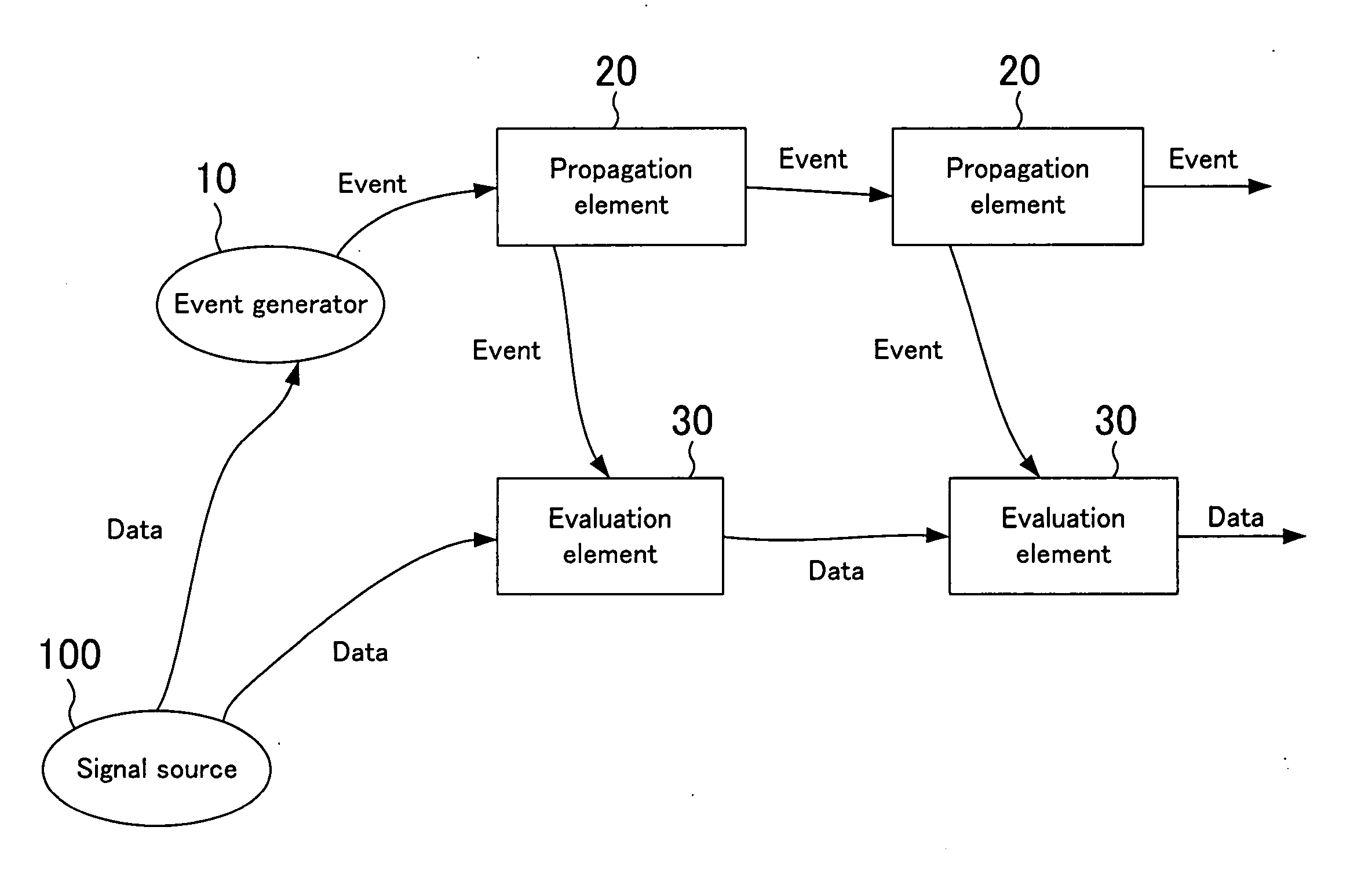
[0077]FIG. 3 shows a general structure of a logic circuit according to embodiment 1 of the present invention. The logic circuit of embodiment 1 includes, as an evaluation element, a storage element 31 for storing input data. The logic circuit of embodiment 1 operates as follows. As the output of a signal source 100 varies, an event is generated by an event generator 10 and propagated through propagation elements 20. A storage element 31 at the first stage stores data output from the signal source 100 based on the event issued by a propagation element 20 at the first stage. The data stored in the storage element 31 at the first stage is subjected to a logical operation of a combinational circuit 32, and a result of the operation is supplied to a storage element 31 at the next stage. The storage element 31 at the next stage stores the data received from the combinational circuit 32 based on the event issued by a corresponding propagation element 20.

[0078] Thus, according to embodimen...

embodiment 2

[0079]FIG. 4 shows a circuit structure of an evaluation element according to embodiment 2 of the present invention. The evaluation element of embodiment 2 includes a capacitor 301, a charge / discharge controller 302 for controlling the charging / discharging of the capacitor 301 with electric charges based on an event, a charging device 303 and a discharging device 304 for charging / discharging the capacitor 301 under the control of the charge / discharge controller 302, an evaluation logic circuit 305 for determining a discharge path by a function, and a static gate 306 (e.g., an inverter). It should be noted that the capacitor 301 is preferably a ferroelectric capacitor.

[0080] Next, an operation of the evaluation element according to embodiment 2 is described with reference to the timing chart of FIG. 5. The charging device 303 operates in response to generation of an event, such that the charge-held state of the capacitor 301 is initialized. Then, the discharging device 304 is activat...

embodiment 3

[0082]FIG. 6 shows a general structure of a logic circuit according to embodiment 3 of the present invention. In the logic circuit of embodiment 3, an evaluation element 30 includes an evaluation controller 40 which receives an event from a propagation element 20 to output various control signals and a substrate bias, and an evaluation section 30′ for evaluating input data under the control of the evaluation controller 40.

[0083]FIG. 7 shows a circuit structure of an evaluation element according to embodiment 3. It should be noted that the evaluation controller is not shown. The evaluation element of embodiment 3 includes a device 303 for controlling a precharge operation based on a given initialization control signal, a device 304 for controlling an evaluation operation based on a given evaluation control signal, an evaluation logic circuit 305 for determining a discharge path by a function, a static gate 306 (e.g., an inverter), and a level keeper 307 for holding a charged / dischar...


PUM


Abstract

A logic circuit comprises: an event generator for detecting a variation in data output from a signal source to generate an event which indicates the variation of the data; a plurality of propagation elements for propagating the event in a chained fashion; and a plurality of evaluation elements for evaluating data received at a first stage from the signal source to propagate a result of the evaluation in a chained fashion. When receiving the event, each of the plurality of evaluation elements evaluates the data input to the evaluation element.

Description

CROSS-REFERENCE TO RELATED APPLICATIONS [0001] This application claims priority under 35 U.S.C. § 119(a) on Japanese Patent Application No. 2004-229842 filed on Aug. 5, 2004 and Japanese Patent Application No. 2005-200003 filed on Jul. 8, 2005, the entire contents of which are hereby incorporated by reference. BACKGROUND OF THE INVENTION [0002] The present invention relates to a logic circuit and specifically to a circuit construction technique for reducing delay and power consumption of a sequential circuit. [0003] Among the presently-existing semiconductor integrated circuits, static circuits, typified by CMOS (Complementary Metal Oxide Semiconductor) circuits, have been widely used. The CMOS circuits have an advantage such that the output does not change so long as the input does not change, and the current consumption includes only a small leak component and an active component which occurs at a value transition, resulting in a relatively small current consumption. On the other ...

Claims


Application Information

Patent Timeline
IPC IPC(8): G06F17/50
CPCH03K19/0963
Inventor SASAGAWA, YUKIHIROTAKAHATA, ATSUSHI
Owner PANASONIC CORP
Features
  • R&D
  • Intellectual Property
  • Life Sciences
  • Materials
  • Tech Scout
  • Unparalleled Data Quality
  • Higher Quality Content
  • 60% Fewer Hallucinations
Learn More