Micro-electronic package structure and method for fabricating the same

a technology of micro-electronic and package structure, which is applied in the direction of electrical equipment, semiconductor devices, and semiconductor/solid-state device details, etc., can solve the problems of reduced stencil cavity size, contact pads, and reduced width of circuits and pads, so as to simplify the overall fabrication process, reduce the overall thickness of the package structure, and improve flexibility

Inactive Publication Date: 2006-03-02
PHOENIX PRECISION TECH CORP
View PDF9 Cites 56 Cited by
  • Summary
  • Abstract
  • Description
  • Claims
  • Application Information

AI Technical Summary

Benefits of technology

[0011] In accordance with the above drawbacks in the prior art, an objective of the present invention is to provide a micro-electronic package structure and a method for fabricating the same, which can integrate of fabrication processes of a chip carrier and semiconductor packaging processes so as to provide greater flexibility in response to the client's requirements as well as simplify fabricating processes of a semiconductor package and the problem of interface integration.
[0012] Another objective of the present invention is to provide a micro-electronic package structure and a method for fabricating the same, which can avoid the problems in the prior art caused by inappropriate electrical connection between a semiconductor chip and a circuit board.
[0013] Still another objective of the present invention is to provide a micro-electronic package structure and a method for fabricating the same, which can simplify the processes of integrating a chip into a circuit board, thereby reducing the process complexity and fabrication cost.
[0014] A further objective of the present invention is to provide a micro-electronic package structure and a method for fabricating the same, which can eliminate the resin flash problem in the prior art, so as to effectively improve the production yield and product reliability.
[0018] Therefore, according to the micro-electronic package structure and the fabrication method thereof in the present invention, at least one semiconductor chip having a plurality of electrode pads formed on at least one surface thereof is provided and received in a cavity of a carrier, with a conductive bump formed on each of the electrode pads. This arrangement can reduce the overall thickness of the package structure in favor of size miniaturization. Moreover, in the present invention, a dielectric layer is formed on the carrier receiving the chip, and conductive structures are formed in the dielectric layer and electrically connected to electrical connection contacts (including the electrode pads and conductive bumps) of the chip, such that the electrical connection contacts of the chip are electrically extended via the conductive structure. This combines the fabrication processes of a chip carrier and the semiconductor packaging processes, thereby providing better flexibility to meet the client's requirements and simplifying the overall fabrication processes as well as solving the problems of interface integration, inappropriate electrical connection and molding encountered in the prior art.
[0019] Furthermore, in response to the problem in the prior art that not all electrode pads of a chip can be electrically extended since they are too densely arranged, the present invention provides a solution by firstly allowing a portion of the electrode pads of the chip to be electrically connected to the first circuit layer via conductive bumps formed on the electrode pads, and allowing the rest of the electrode pads to be electrically connected to the second circuit layer via the conductive bumps and conductive structures formed through the dielectric layers, such that electrical connection between the chip and the carrier or circuit board can be established.

Problems solved by technology

However, in such packages, both the width of circuits and the size of pads are miniaturized.
This not only cause an alignment problem for subsequently forming pre-solder bumps on the pads, but also makes stencil cavitys being reduced in size thereby causing the solder material difficult to deposit on the pads (contact pads) due to the space occupied by the protective layer.
As a result, the stencil printing technique would have extremely low yield and cannot be employed.
Moreover, the cost of the stencil is increased due to reduction of pad size and pad pitch, making the overall fabrication cost raised.
Furthermore, with the pitch distance between the adjacent pads being reduced, the contact surface area between the protective layer and the circuit board becomes even smaller, thereby diminish the adhesion between the protective layer and the circuit board.
This not only increases the fabrication process complexity and cost, but also leads to the reliability concern.
Regardless of the use of the flip-chip packaging technology or the wire-bonding packaging technology, fabrication of the circuit board and packaging of the semiconductor chip require different machines and procedures, thereby making the fabrication processes very complicated and costly.
However, in practice, the mold is often limited to a particular design of the semiconductor package, such that the size of a molding cavity and the clamping positions may bear structural differences and are not able to tightly clamp the circuit board.
When the epoxy resin in injected into the molding cavity, these differences may lead to a resin flash problem that resin may flash to the surface of the circuit board.
As a result, the surface planarity and appearance of the semiconductor package would both be damaged, and ball pads on the circuit board for subsequently bonding solder balls may be contaminated, such that the quality of electrical connection as well as the yield and reliability of the semiconductor package are seriously degraded.
Since the fabrication processes of the semiconductor device involve a number of different manufacturers, including the carrier manufacturer and the semiconductor packaging manufacturer, the fabrication processes are complicated in practice and not easy to achieve interface integration.
In case the client wishes to modify the product design, the changes and integration involved are even more complicated, not meeting the requirements of flexibility in change and economical benefit.

Method used


Image

  • Micro-electronic package structure and method for fabricating the same
  • Micro-electronic package structure and method for fabricating the same
  • Micro-electronic package structure and method for fabricating the same

Examples


Embodiment Construction

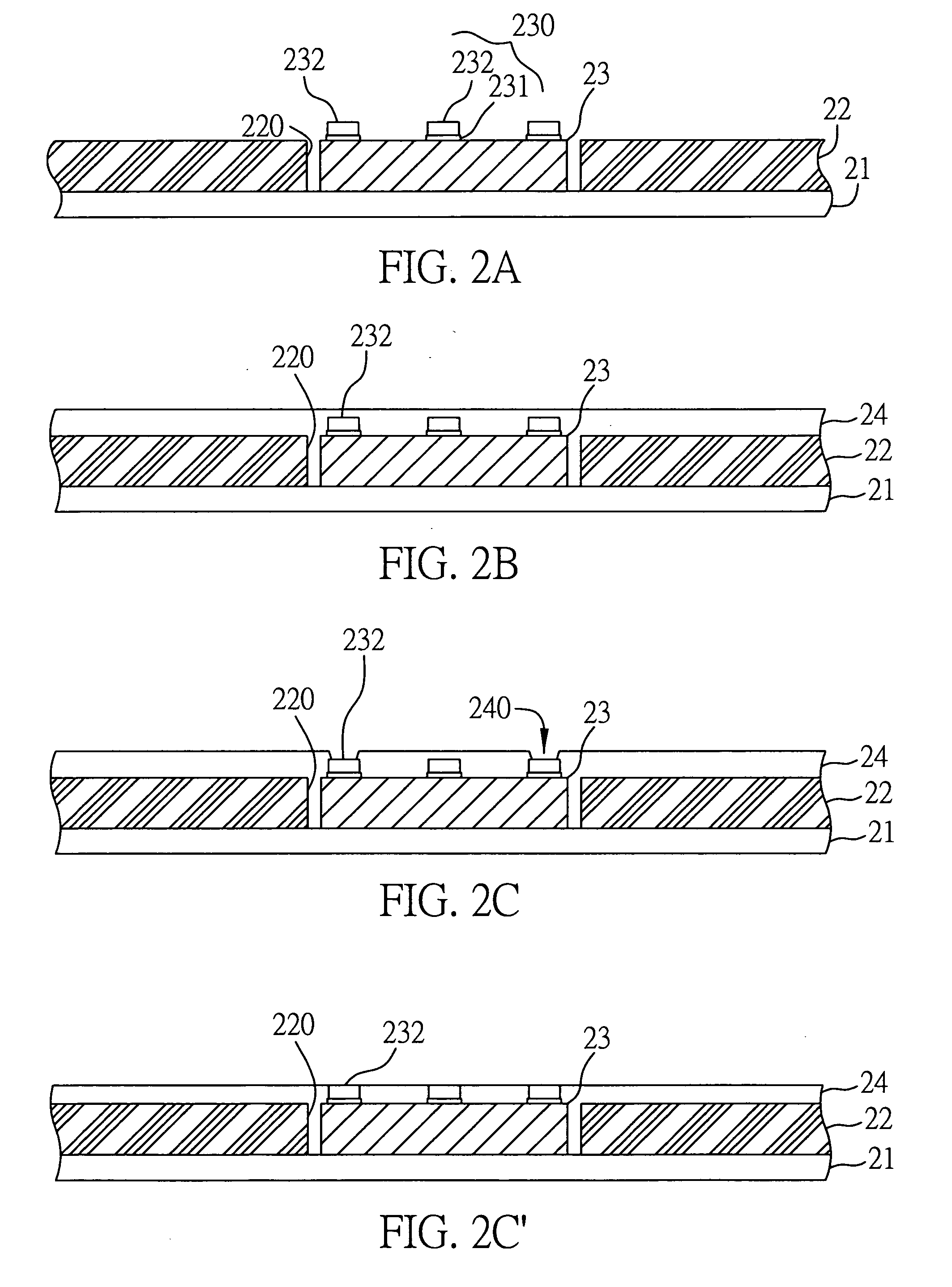
[0025]FIGS. 2A to 2F show the procedural steps of a method for fabricating a micro-electronic package structure in accordance with the present invention.

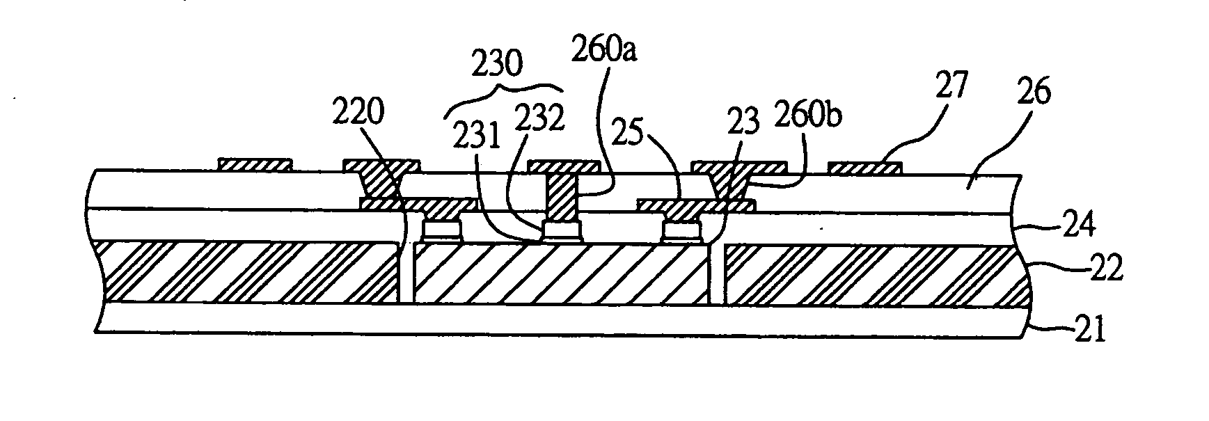
[0026] Referring to FIG. 2A, a carrier 22 is provided, which can be a metal board, insulating board, or circuit board. The carrier 22 is formed with at least one cavity 220 therethrough. A supporting member 21 may be attached on one side of the carrier 22 and covers one end of the cavity 220. This supporting member 21 can be an adhesive layer or a metal layer, which allows at least one semiconductor chip 23 to be mounted the supporting member 21 and received in the cavity 220 of the carrier 22, wherein electrical connection contacts 230 formed on an active surface of the chip 23 are exposed to the cavity 220. The electrical connection contacts 230 of the chip 23 comprise electrode pads 231 and conductive bumps 232 formed on the electrode pads 231, and are used to establish good external electrical connection for the chip 23.

[0027]...


PUM


Abstract

A micro-electronic package structure and a method for fabricating the same are proposed. A carrier is prepared and provided with a cavity for receiving at least one semiconductor chip having a plurality of electrical connection contacts. A dielectric layer is formed on the carrier, with the electrical connection contacts being exposed from the dielectric layer. A first circuit layer is formed on the dielectric layer and electrically connected to a portion of the electrical connection contacts of the chip. Another dielectric layer is formed on the first circuit layer and said dielectric layer, and a second circuit layer is formed on this dielectric layer and electrically connected to the rest of the electrical connection contacts of the chip and the first circuit layer by conductive vias, such that the chip is integrated into the carrier.

Description

FIELD OF THE INVENTION [0001] The present invention relates to micro-electronic package structures and methods for fabricating the same, and more particularly to a circuit board integrated with a semiconductor chip, and a method for fabricating the circuit board structure. BACKGROUND OF THE INVENTION [0002] As the semiconductor packaging technology advances, there have been developed many different types of semiconductor packages. One of the advanced semiconductor packages is referred to as ball grid array (BGA) package, which is characterized in using a substrate for accommodating a chip on a front surface thereof, and implanting a plurality of array-arranged solder balls on a back surface of the substrate via a self-alignment technique. This arrangement allows relatively more solder balls to be incorporated on a unit area of the substrate acting as a chip carrier, which is desirable for a highly integrated semiconductor chip, and the solder balls serve as I / O (input / output) connec...

Claims


Application Information

Patent Timeline
Patent Type & Authority Applications(United States)
IPC IPC(8): H01L23/02
CPCH01L24/19H01L2924/01033H01L2224/04105H01L2224/20H01L2224/24227H01L2924/01029H01L2924/01079H01L2924/01082H01L2924/14H01L2924/15153H01L2924/1517H01L2224/0401H01L2224/73204H01L2224/32225H01L2224/16225H01L24/24H01L2924/00H01L2224/73267
Inventor HSU, SHIH-PING
Owner PHOENIX PRECISION TECH CORP
Why Eureka
Try Eureka