Method of fabricating semiconductor a device

a semiconductor and manufacturing method technology, applied in the field of semiconductor devices, can solve the problems of time-dependent changes in threshold voltage, shorten gate length, increase non-conformities, etc., and achieve the effect of simple and exact, improved threshold voltage and current drivability, and high device integration

Inactive Publication Date: 2006-03-02
FUJITSU SEMICON LTD
View PDF6 Cites 8 Cited by
  • Summary
  • Abstract
  • Description
  • Claims
  • Application Information

AI Technical Summary

Benefits of technology

[0015] The present invention is completed for solving the foregoing problems, and is to provide a semiconductor device and a method of fabricating thereof whereby shrinkage and higher integration of the device can be ensured in a simple and exact manner without ruining an effort to improve roll-off characteristic of the threshold voltage and current drivability and to reduce drain leakage current; and is in particular to provide a CMOS-structured semiconductor device and a method of fabricating thereof whereby optimum design of the device can be ensured so as to realize advanced performance and lowered power consumption.

Problems solved by technology

Shortening of the gate length, however, tends to raise nonconformities such as time-dependent changes in the threshold voltage due to hot carriers and degradation of mutual conductance.
Recent accelerated trends towards still higher shrinkage and still higher integration of MOS transistors have, however, raised two following problems in those having the extension structure.
It is, however, extremely difficult to desirably control the sharpness in the profile since the lateral concentration profile is generally governed by diffusion phenomenon.
They are, however, heavy elements and thus causative of crystal defects when they are introduced by ion implantation, which defects cannot completely be removed even after annealing for activation, and tend to increase drain leakage, especially its component around the gate electrode.
While annealing for clearing defects is known to be effective for suppressing the drain leakage current, the annealing also promotes diffusion of the impurities, which interferes shrinkage of the device.
As described in the above, an effort to further shrink the extension-structured MOS transistors undesirably makes it difficult to control the lateral concentration profile in the extension region, and an additional effort to form the pocket region aimed at improving roll-off characteristic of the threshold voltage and current drivability through reduction in drain leakage current undesirably makes it difficult to shrink the device, which is against the major purpose of the process.

Method used


Image

  • Method of fabricating semiconductor a device
  • Method of fabricating semiconductor a device
  • Method of fabricating semiconductor a device

Examples


specific embodiments

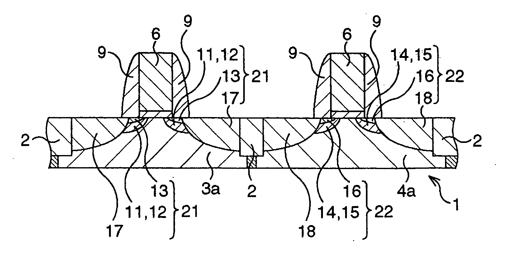
[0048] Based on the basic concept of the present invention described in the above, specific embodiments will be explained. The following paragraphs exemplify a CMOS transistor as a semiconductor device, and therefore deal with constitutions thereof together with methods of fabricating thereof. It is to be noted that the present invention is by no means limited to CMOS transistor, but is applicable to any semiconductor devices based on transistor structure having a gate, source and drain.

first embodiment

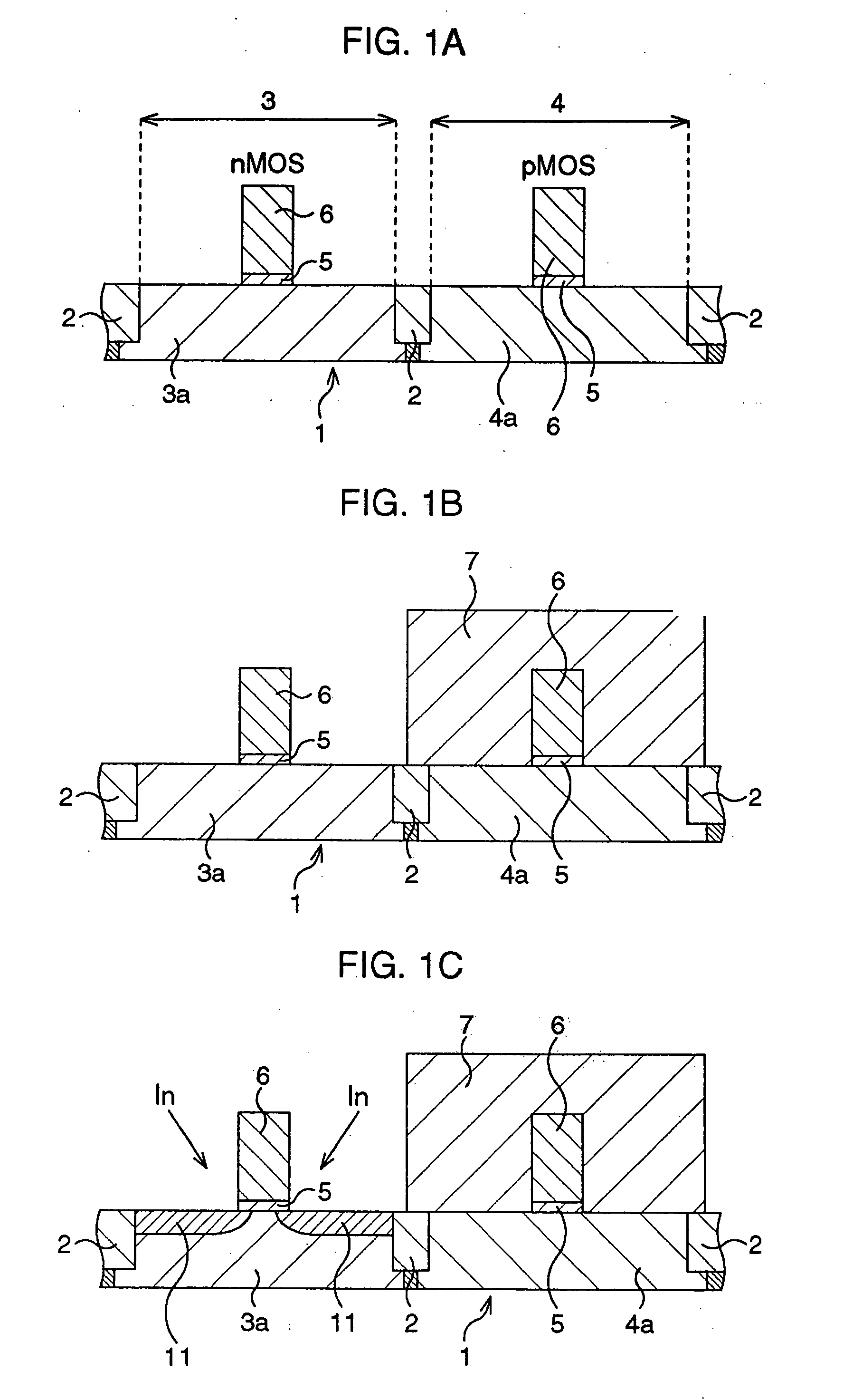
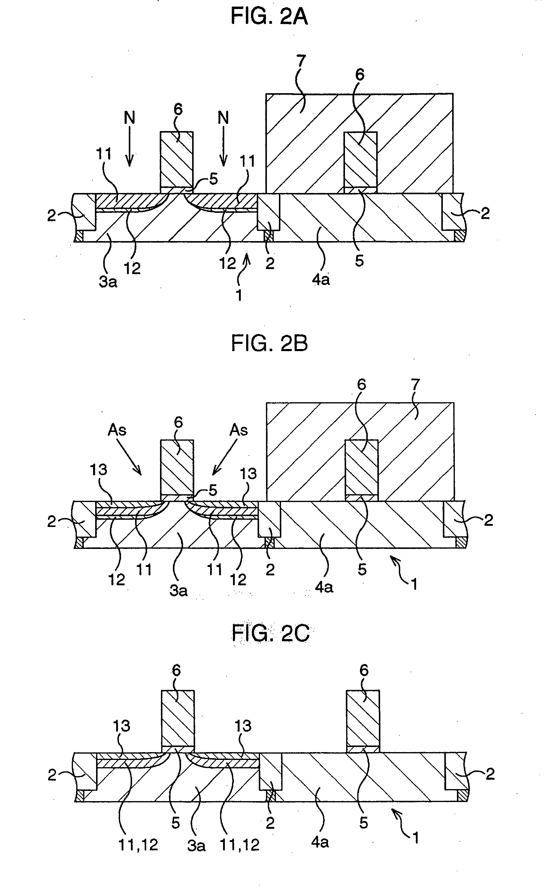
[0049]FIGS. 1A through 4C are schematic sectional views serially showing process steps of a method of fabricating a CMOS transistor according to the first embodiment.

[0050] First as shown in FIG. 1A, element active regions and gate electrodes are formed according to general CMOS processes.

[0051] More specifically, according to STI (shallow trench isolation) process, trenches are formed by photolithography and dry etching in a semiconductor substrate 1 in the areas planned for forming element isolation region, a silicon oxide film is deposited typically by CVD process so as to fill the trenches, and the silicon oxide film is removed by CMP (chemical mechanical polishing) from the top so as to allow it to remain only in the trenches, to thereby form STI-type element isolation structure 2 and partition an n-type element active region 3 and a p-type element active region 4. Next, a p-type impurity and an n-type impurity are introduced by ion implantation into the n-type element active...

second embodiment

[0088] In the second embodiment, a special consideration is made on formation of the pocket layer of an nMOS transistor in a CMOS transistor, whereby a diffusion-suppressive substance was introduced only to the nMOS transistor.

[0089]FIGS. 8A through 11C are schematic sectional views serially showing process steps of a method of fabricating a CMOS transistor according to the second embodiment.

[0090] First as shown in FIG. 8A, element active regions and gate electrodes are formed according to general CMOS processes.

[0091] More specifically, according to STI (shallow trench isolation) process, trenches are formed by photolithography and dry etching in a semiconductor substrate 1 in the areas planned for forming element isolation region, a silicon oxide film is deposited typically by CVD process so as to fill the trenches, and the silicon oxide film is removed by CMP (chemical mechanical polishing) from the top so as to allow it to remain only in the trenches, to thereby form STI-typ...


PUM


Abstract

An impurity-diffused layer having an extension structure is formed first by implanting Sb ion as an impurity for forming a pocket region; then by implanting N as a diffusion-suppressive substance so as to produce two peaks in the vicinity of the interface with a gate electrode and at an amorphous / crystal interface which serves as an defect interface generated by the impurity in the pocket region; and by carrying out ion implantations for forming an extension region and deep source and drain regions.

Description

CROSS-REFERENCE TO RELATED APPLICATIONS [0001] This application is based upon and claims the benefit of priority from the prior Japanese Patent Application Nos. 2002-183055, filed on Jun. 24, 2002, 2002-355884, filed on Dec. 6, 2002 and 2003-168799, filed on Jun. 13, 2003, the entire contents of which are incorporated herein by reference. BACKGROUND OF THE INVENTION [0002] 1. Field of the Invention [0003] This invention relates to a semiconductor device having an extension structure and a method of fabricating thereof, which are particularly preferable as being applied to CMOS-structured semiconductor device. [0004] 2. Description of the Related Art [0005] Many conventional MOS transistors employ LDD structure in order to suppress short channel effect and to improve hot-carrier resistance. [0006] On the other hand, a major stream towards higher shrinkage and higher integration has been shortening gate length of MOS transistors. Shortening of the gate length, however, tends to raise ...

Claims


Application Information

Patent Timeline
Patent Type & Authority Applications(United States)
IPC IPC(8): H01L21/8238H01L21/265H01L21/336H01L27/092H01L29/78
CPCH01L21/26506H04W4/24H01L21/823807H01L21/823814H01L29/66492H01L29/6656H01L29/6659H04M15/8016H04M15/81H04M2215/0112H04M2215/2026H04M2215/22H04M2215/32H04M2215/7414H01L21/26586H01L21/2658H01L27/092H01L21/26513
Inventor MOMIYAMA, YOUICHIOKABE, KENICHISAIKI, TAKASHIFUKUTOME, HIDENOBU
Owner FUJITSU SEMICON LTD
Why Eureka
Try Eureka