

Method for forming a nanocrystal floating gate for a flash memory device
a technology of floating gate and flash memory, which is applied in the direction of nanotechnology, semiconductor devices, electrical devices, etc., can solve the problems of device leakage, loss of cell charge, and decrease of doping density, so as to achieve more controllability and improve uniformity
- Summary
- Abstract
- Description
- Claims
- Application Information
AI Technical Summary
Benefits of technology
Problems solved by technology
Method used
Image

Examples
Embodiment Construction
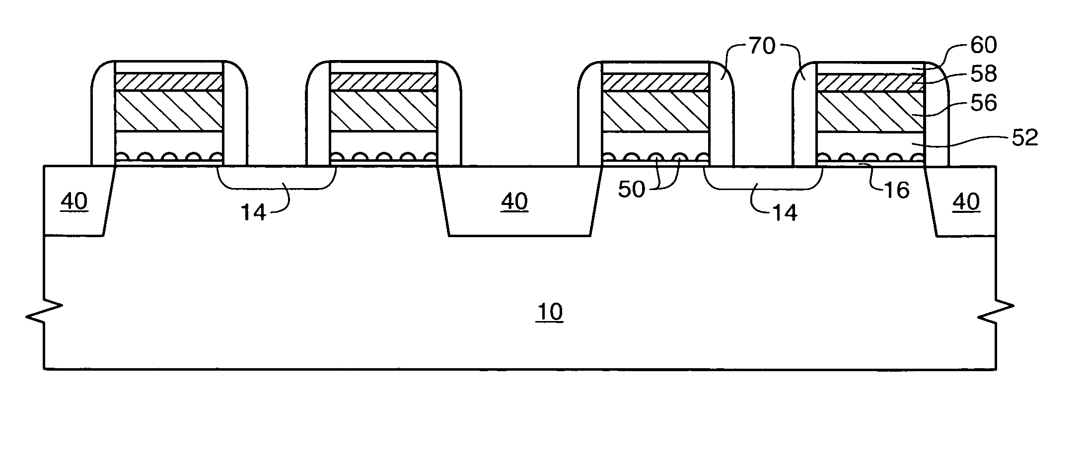
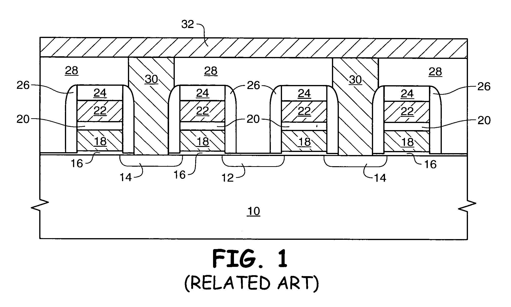
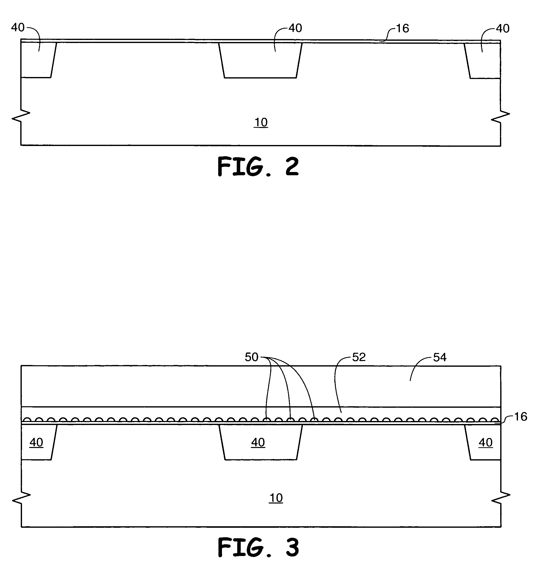
[0019] The term “wafer” is to be understood as a semiconductor-based material including silicon, silicon-on-insulator (SOI) or silicon-on-sapphire (SOS) technology, doped and undoped semiconductors, epitaxial layers of silicon supported by a base semiconductor foundation, and other semiconductor structures. Furthermore, when reference is made to a “wafer” in the following description, previous process steps may have been utilized to form regions or junctions in or over the base semiconductor structure or foundation. Additionally, when reference is made to a “substrate assembly” in the following description, the substrate assembly may include a wafer with layers including dielectrics and conductors, and features such as transistors, formed thereover, depending on the particular stage of processing. In addition, the semiconductor need not be silicon-based, but could be based on silicon-germanium, silicon-on-insulator, silicon-on-sapphire, germanium, or gallium arsenide, among others. ...
PUM
 Abstract
Description
Claims
Application Information