Thin film transistor array panel and method for manufacturing the same

a technology of thin film transistors and array panels, which is applied in the field of thin film transistor array panels and the field of manufacturing the same, can solve the problems of high stress and resistivity, poor contact between drain electrodes of al and pixel electrodes of ito, and cr is not suitable for use in a large size lcd, etc., and achieves low resistivity, good contact characteristics, and low resistance.

Inactive Publication Date: 2006-03-09
SAMSUNG DISPLAY CO LTD
View PDF4 Cites 39 Cited by
  • Summary
  • Abstract
  • Description
  • Claims
  • Application Information

AI Technical Summary

Benefits of technology

[0013] It is an object of the present invention to solve the above-mentioned problems and to provide a thin film transistor array panel with signal lines having low resistivity and good contact characteristics without such problems.
[0014] To achieve the object, the present invention provides a thin film transistor array panel having gate lines and data lines formed of molybdenum alloy (Mo-alloy), which is composed of Mo and at least one of niobium (Nb), vanadium (V), and titanium (Ti), and has low resistivity and good chemical resistance.

Problems solved by technology

However, Cr includes the drawbacks of high stress and resistivity.
Accordingly, Cr is not appropriate for use in a large size LCD.
However, Al also has drawbacks including hillock growth that may be induced by high temperature, Al may be diffused into a semiconductor when Al contacts the semiconductor, and, since Al has poor contact characteristics with pixel electrode materials, such as indium tin oxide (ITO), a poor contact between a drain electrode of Al and a pixel electrode of ITO may occur.

Method used


Image

  • Thin film transistor array panel and method for manufacturing the same
  • Thin film transistor array panel and method for manufacturing the same
  • Thin film transistor array panel and method for manufacturing the same

Examples


embodiment 1

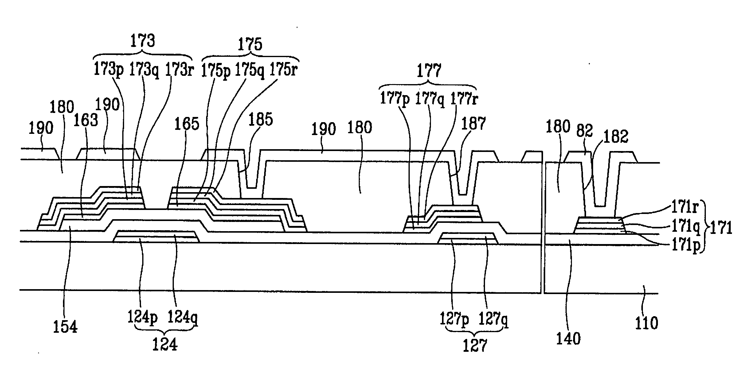
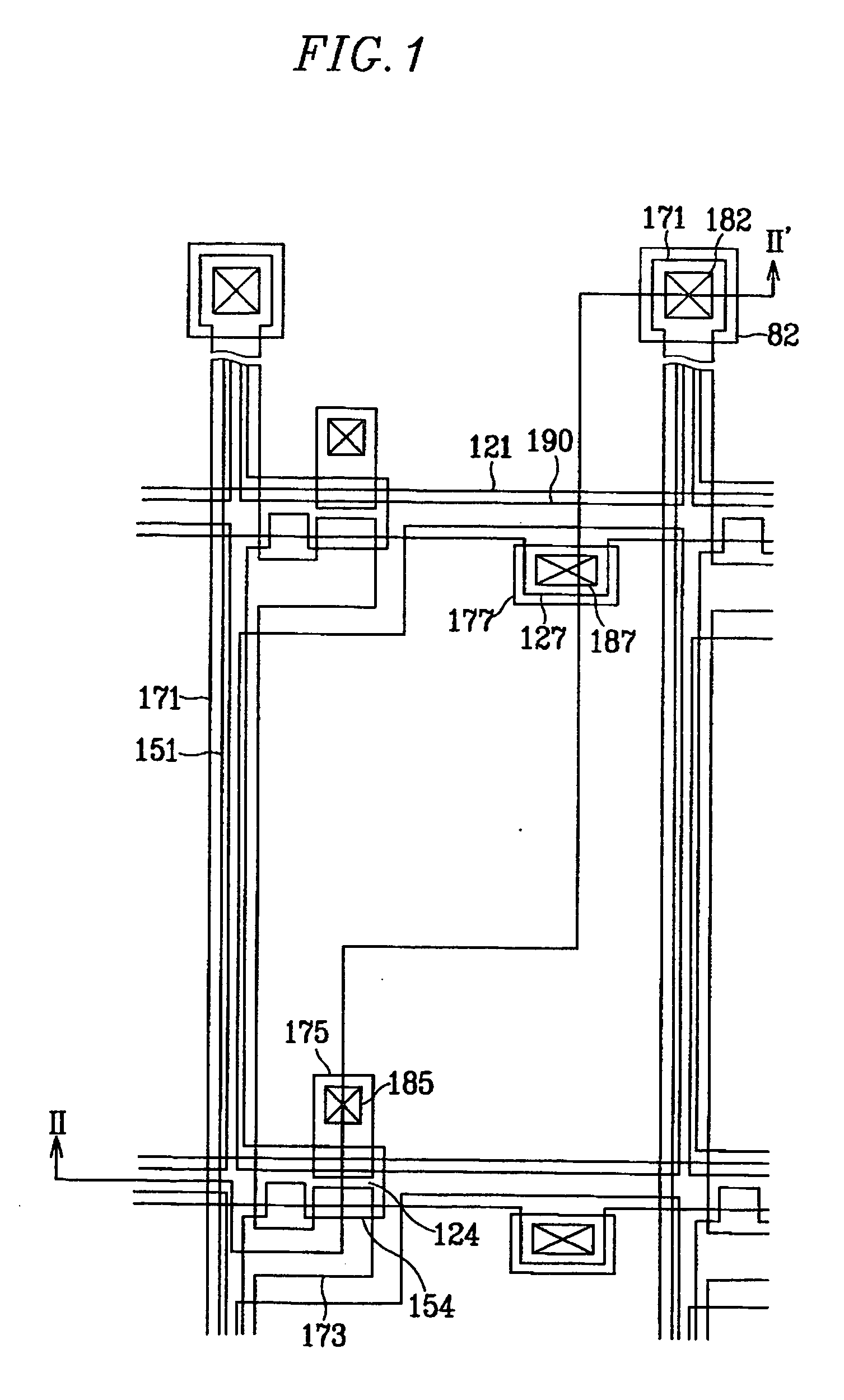
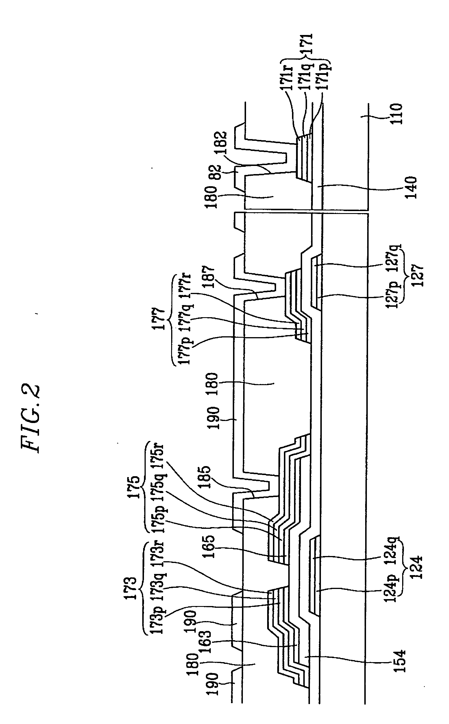
[0048] At first, a TFT array panel for an LCD according to a first embodiment of the present invention will be described in detail with reference to FIGS. 1 and 2.

[0049]FIG. 1 is a layout view of a TFT array panel for an LCD according to an embodiment of the present invention and FIG. 2 is a sectional view of the TFT array panel shown in FIG. 1 taken along the line II-II.

[0050] A plurality of gate lines 121 for transmitting gate signals are formed on an insulating substrate 110. The gate lines 121 are mainly formed in the horizontal direction and partial portions thereof become a plurality of gate electrodes 124. Also, different partial portions thereof that extend in a lower direction become a plurality of expansions 127.

[0051] The gate line 121 has lower layers 124p and 127p and upper layers 124q and 127q. The lower layers 124p and 127p are made of Al or an aluminum alloy such as aluminum-neodymium (Al—Nd). The upper layers 124q and 127q are made of a molybdenum alloy (Mo-alloy...

embodiment 2

[0102] The data lines and the semiconductors are formed by different photo etching processes using different photo masks than in the first embodiment. However, the data lines and the semiconductors may be simultaneously formed by a photo etching process using a same photo mask to reduce production costs. Such an embodiment will be described in detail with reference to the drawings.

[0103]FIG. 7 is a layout view of a TFT array panel for an LCD according to another embodiment of the present invention. FIG. 8 is a sectional view of the TFT array panel shown in FIG. 7 taken along the line VIII-VIII′.

[0104] Referring to FIGS. 7 and 8, a plurality of gate lines 121, including a plurality of gate electrodes 124 and a plurality of storage electrode lines 131 which are electrically separated from the gate lines 121, are formed on a substrate 110.

[0105] The gate lines 121 and the storage electrode lines 131 have lower layers 121p and 131p and upper layers 121q and 131q. The lower layers 121...

embodiment 3

[0140] The present embodiment illustrates a thin film transistor (TFT) array panel having color filters.

[0141]FIG. 14A is a layout view of a TFT array panel for an LCD according to another embodiment of the present invention. FIG. 14B is a sectional view of the TFT array panel shown in FIG. 14A taken along the line XIVB-XIVB′.

[0142] A plurality of gate lines 121 for transmitting gate signals are formed on an insulating substrate 110. The gate lines 121 are mainly formed in the horizontal direction and the partial portions thereof become a plurality of gate electrodes 124. Also, different partial portions thereof, which extend in a lower direction, become a plurality of expansions 127.

[0143] The gate line 121 has lower layers 124p and 127p and upper layers 124q and 127q. The lower layers 124p and 127p are made of aluminum (Al) or an aluminum alloy such as aluminum-neodymium (Al—Nd). The upper layers 124q and 127q are made of a molybdenum alloy (Mo-alloy: Mo—Nb, Mo—V, Mo—Ti), which...


PUM

PropertyMeasurementUnit
inclination angleaaaaaaaaaa
inclination anglesaaaaaaaaaa
dielectric constantaaaaaaaaaa

Abstract

The present invention provides a TFT array panel and a manufacturing method of the same, which has signal lines including a lower layer of an Al containing metal and an upper layer of a molybdenum alloy (Mo-alloy) comprising molybdenum (Mo) and at least one of niobium (Nb), vanadium (V), and titanium (Ti). Accordingly, undercut, overhang, and mouse bites which may arise in an etching process, are prevented, and TFT array panels that have signal lines having low resistivity and good contact characteristics are provided.

Description

CROSS-REFERENCE TO RELATED APPLICATION [0001] This application claims priority to a corresponding patent application 10-2004-0071612 filed in the Korean Intellectual Property Office, Republic of Korea, on Sep. 8, 2004, the entire content of which is hereby incorporated by reference. BACKGROUND OF THE INVENTION [0002] (a) Field of the Invention [0003] The present description relates to a thin film transistor (TFT) array panel for a liquid crystal display (LCD) or an organic light emitting display (OLED) and a manufacturing method for the same. [0004] (b) Description of the Related Art [0005] Liquid crystal displays (LCDs) are one of the most widely used flat panel displays. An LCD includes a liquid crystal (LC) layer interposed between two panels provided with field-generating electrodes. The LCD displays images by applying voltages to the field-generating electrodes to generate an electric field in the LC layer that determines orientations of LC molecules in the LC layer to adjust t...

Claims


Application Information

Patent Timeline
Patent Type & Authority Applications(United States)
IPC IPC(8): G02F1/136
CPCG02F1/136286G02F2001/13629Y10S438/924H01L27/3276G02F2001/136295G02F1/13629G02F1/136295H10K59/131G02F1/136
Inventor CHO, BEOM-SEOKBAE, YANG-HOLEE, JE-HUNJEONG, CHANG-OH
Owner SAMSUNG DISPLAY CO LTD
Why Eureka
Try Eureka