Processes for producing Bi12MO20 precursors, Bi12MO20 particles, and photo-conductor layers

a technology of photoconductor layer and precursor, which is applied in the direction of titanium compounds, chemistry apparatus and processes, solid-state devices, etc., can solve the problems of low speed, low contrast in a low dose region, and large dark current, so as to achieve enhanced effect of collecting formed electric charges, high purity, and uniform composition

Inactive Publication Date: 2006-03-09
FUJIFILM CORP +1
View PDF5 Cites 13 Cited by
  • Summary
  • Abstract
  • Description
  • Claims
  • Application Information

AI Technical Summary

Benefits of technology

[0060] Further, the second process for producing Bi12MO20 particles in accordance with the present invention has the advantages described below over the conventional solid phase technique, wherein Bi2O3 and the metal oxide are subjected to the firing processing, and wherein the Bi12MO20 particles are thereby synthesized. Specifically, with the second process for producing Bi12MO20 particles in accordance with the present invention, the Bi12MO20 precursor, which has the uniform composition, is subjected to the firing processing. Therefore, the Bi12MO20 particles having the uniform composition are capable o...

Problems solved by technology

However, ordinarily, amorphous selenium has the problems in that it is necessary for the layer thickness of the photo-conductor layer to be set to be large (e.g., at least 500 μm) because of a low radiation absorptivity.
However, if the layer thickness of the photo-conductor layer is set to be large, the problems will occur in that the speed, with which the electrostatic latent image is read out, becomes low.
Also, the problems will occur in that, since a high voltage is applied across the photo-conductor layer at least during a period from the beginning of the read-out operation after the formation of the electrostatic latent image to the end of the read-out operation, a dark current becomes large, electric charges occurring due to the dark current are added to the latent image charges, and the contrast in a low dose region becomes low.
Further, since the high voltage is applied across the photo-conductor layer, device deterioration is apt to occur, durability becomes low, and electric noise is apt to occur.
Therefore, considerable time is required to grow the photo-conductor layer up to the large layer thickness described above with the vacuum evaporation technique, and management of the growth of the photo-conductor layer is not easy to perform.
As a result, the production cost of the photo-conductor layer is not capable of being kept low, and the cost ...

Method used


Image

  • Processes for producing Bi12MO20 precursors, Bi12MO20 particles, and photo-conductor layers
  • Processes for producing Bi12MO20 precursors, Bi12MO20 particles, and photo-conductor layers
  • Processes for producing Bi12MO20 precursors, Bi12MO20 particles, and photo-conductor layers

Examples


examples i

Example 1

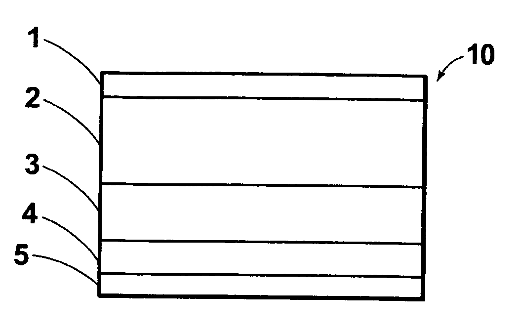
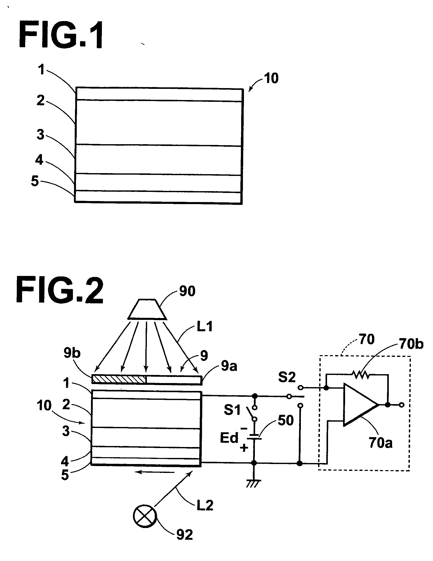
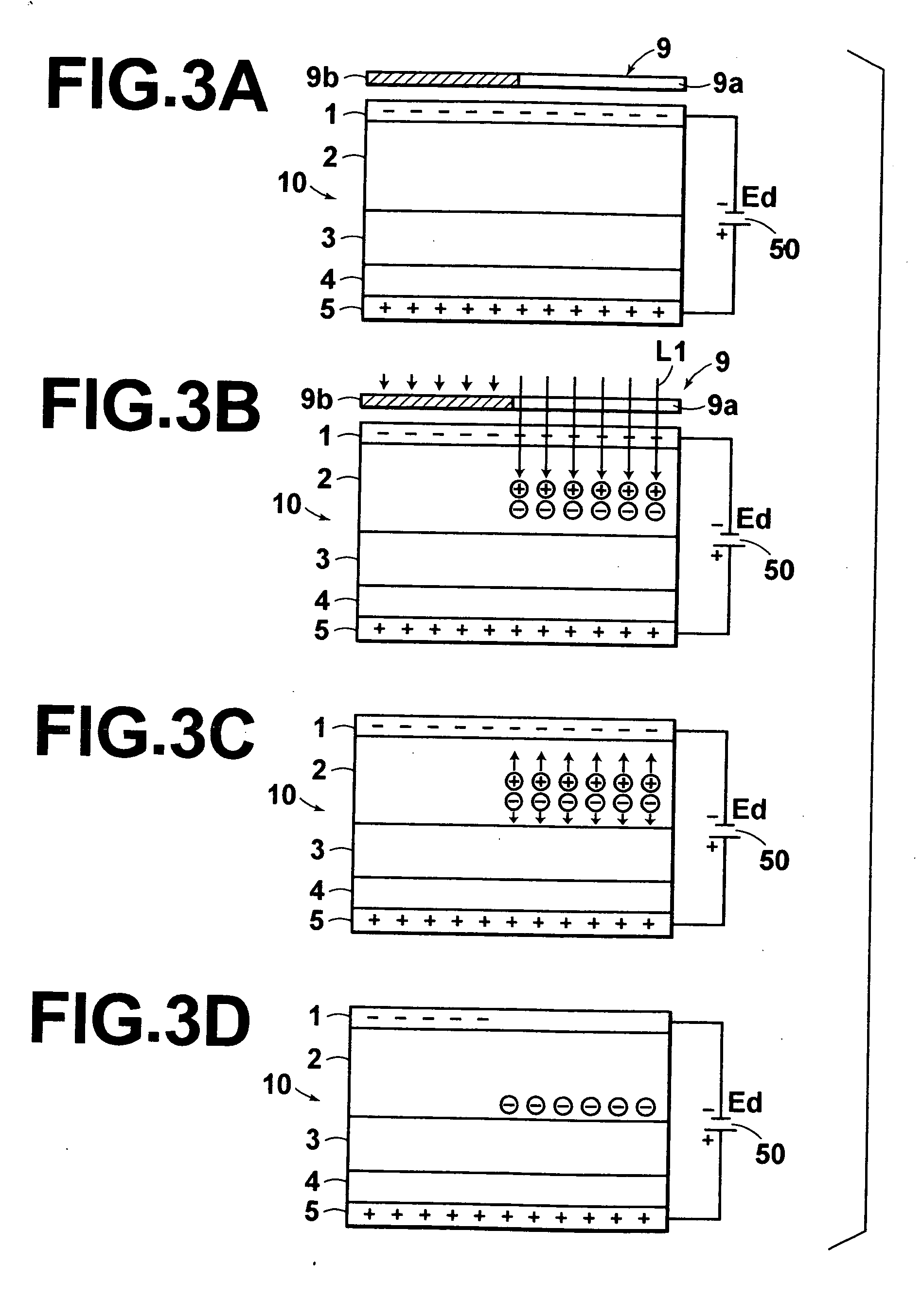
[0126] An aqueous NH3 solution (28% by weight) was added to a mixed methoxy ethanol solution of 5N Bi(NO3)3.5H2O and 6N Ti(O-i-C3H7)4, and a Bi12TiO20 precursor was thereby obtained. The thus obtained Bi12TiO20 precursor was subjected to molding processing with a uniaxial press (10 MPa˜140 MPa) and thereafter subjected to CIP molding processing (200 MPa˜700 MPa). The thus molded B12TiO20 precursor was then subjected to firing processing in an ambient atmosphere at a temperature of 800° C. for two hours and under an Ar flow condition, and a Bi12TiO20 fired film was thereby formed. The Bi12TiO20 fired film was then adhered to an ITO base plate by use of a silver paste. Thereafter, an Au layer acting as a top electrode was formed with sputtering processing to a thickness of 60 nm on the Bi12TiO20 fired film, which had been adhered to the ITO base plate. In this manner, a radiation imaging panel, which was provided with a photo-conductor layer constituted of the Bi12TiO20 fire...

example 2

[0127] A radiation imaging panel, which was provided with a photo-conductor layer constituted of a Bi12SiO20 fired film, was obtained in the same manner as that in Example 1, except that, in lieu of Ti(O-i-C3H7)4 utilized in Example 1, Si(O—C2H5)4 was utilized.

example 3

[0128] A radiation imaging panel, which was provided with a photo-conductor layer constituted of a Bi12GeO20 fired film, was obtained in the same manner as that in Example 1, except that, in lieu of Ti (O-i-C3H7)4 utilized in Example 1, Ge(O—C2H5)4 was utilized.


PUM


Abstract

A mixed solution of a bismuth salt and a metal alkoxide is mixed together with an aqueous alkali solution, and a Bi12MO20 precursor, in which M represents at least one kind of element selected from the group consisting of Ge, Si, and Ti, is thereby obtained. The Bi12MO20 precursor is subjected to molding processing, the thus molded Bi12MO20 precursor is subjected to firing processing, and a photo-conductor layer is thereby produced. Alternatively, the Bi12MO20 precursor is subjected to heating processing in an alkaline liquid phase or to firing processing, and Bi12MO20 particles are thereby obtained. A photo-conductor layer is produced by use of the thus obtained Bi12MO20 particles.

Description

BACKGROUND OF THE INVENTION [0001] 1. Field of the Invention [0002] This invention relates to a process for producing a Bi12MO20 precursor. This invention also relates to a process for producing Bi12MO20 particles, which are suitable for use in a photo-conductor layer for constituting a radiation imaging panel. This invention further relates to a process for producing a photo-conductor layer for constituting a radiation imaging panel. [0003] 2. Description of the Related Art [0004] There have heretofore been proposed X-ray imaging panels designed for use in a medical X-ray image recording operation, such that a radiation dose delivered to an object during the medical X-ray image recording operation may be kept small, and such that the image quality of an image and its capability of serving as an effective tool in, particularly, the efficient and accurate diagnosis of an illness may be enhanced. With the proposed X-ray imaging panels, a photo-conductor layer sensitive to X-rays is em...

Claims


Application Information

Patent Timeline
IPC IPC(8): C01G23/00
CPCC01G29/00H01L31/085H01L27/14658
Inventor KAITO, RYOUZOU
Owner FUJIFILM CORP
Why Eureka
Try Eureka