Nitride semiconductor light emitting device and method of manufacturing the same

a light-emitting device and semiconductor technology, applied in the direction of lifting devices, semiconductor devices, electrical equipment, etc., can solve the problems of increasing the operating voltage of the device, increasing heat generation, and difficulty in achieving ohmic contact with the electrodes therein, so as to reduce contact resistance, enhance the efficiency of electric current distribution, and high electron mobility

Active Publication Date: 2006-03-16
SAMSUNG ELECTRONICS CO LTD
View PDF7 Cites 24 Cited by
  • Summary
  • Abstract
  • Description
  • Claims
  • Application Information

AI Technical Summary

Benefits of technology

[0014] The present invention has been made in view of the above problems, and it is an object of the present invention to provide a high brightness nitride semiconductor light emitting device, which has a two-dimensional electron gas (2DEG) layer formed on a p-type clad layer having a p-side electrode formed thereon, thereby enhancing contact resistance and electric current injection efficiency.
[0023] As such, according to the present invention, the two-dimensional electron gas (2DEG) layer is formed adjacent to a portion formed with the p-side electrode in order to reduce contact resistance. Particularly, the 2DEG layer has remarkably high electron mobility, thereby significantly enhancing the electric current distribution efficiency.

Problems solved by technology

However, since the nitride semiconductor has a relatively large energy band gap, there is a difficulty in achieving an ohmic contact with electrodes therein.
Particularly, contact resistance between a p-side electrode and a p-type nitride semiconductor is increased due to the larger energy band gap of the p-type- nitride semiconductor, thereby increasing the operating voltage of the device, which results in an increase of heat generation thereof.
Additionally, since a portion formed with the p-side electrode acts as a main light-emitting surface in a typical non-flip chip structure, the above method for enhancing the ohmic contact has a technological restriction in that transmission of light must be ensured.
In order to ensure high transmittance, the thickness (100 μm) of the Ni / Au transparent electrode must be restricted, causing a limitation in sufficient enhancement of the electric current injection efficiency.
However, an excessive amount of the p-type impurity causes reduction of crystallinity.

Method used


Image

  • Nitride semiconductor light emitting device and method of manufacturing the same
  • Nitride semiconductor light emitting device and method of manufacturing the same
  • Nitride semiconductor light emitting device and method of manufacturing the same

Examples


Embodiment Construction

[0029] Preferred embodiments of the present invention will now be described in detail with reference to the accompanying drawings.

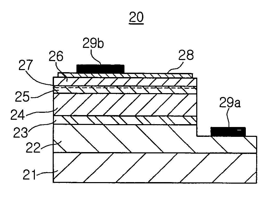
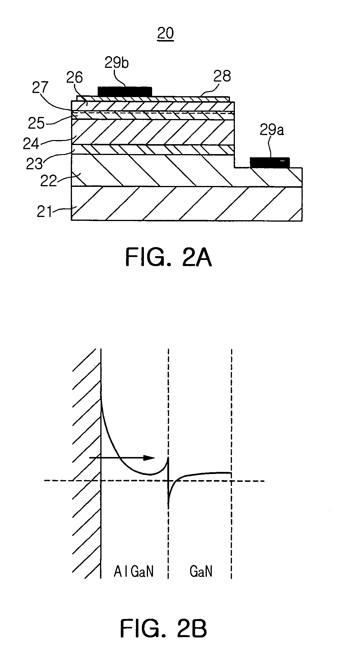
[0030]FIG. 2a is a sectional side elevation illustrating a nitride semiconductor light emitting device according to one embodiment of the present invention, and FIG. 2b shows an energy band structure of AlGaN / GaN layers of the nitride semiconductor light emitting device shown in FIG. 2a.

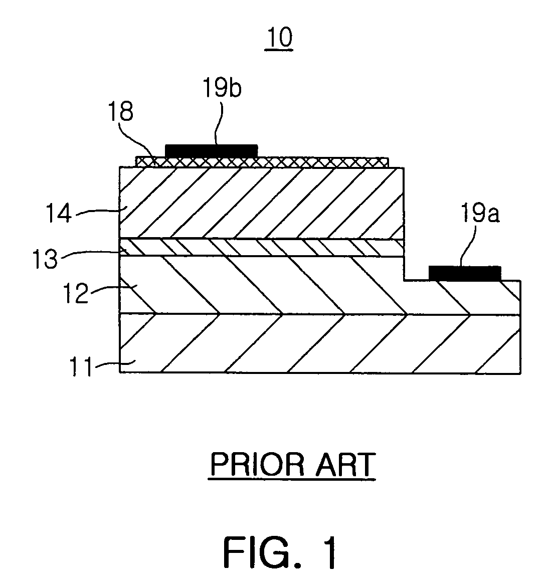
[0031] Referring to FIG. 2a, similar to the light emitting device 10 shown in FIG. 1, a nitride semiconductor light emitting device 20 according to the embodiment of the present invention comprises an n-type nitride layer 22, an active layer 23, and a p-type GaN nitride layer 24, which are sequentially formed on a sapphire substrate 21 in this order. The p-type and n-type nitride semiconductor layers 22 and 24 may be a GaN layer and a GaN / AlGaN layer, each having a conductive impurity doped therein, respectively. The active layer 23 may have a multi-quantum well structur...


PUM


Abstract

A nitride semiconductor light emitting device and a method of manufacturing the same are disclosed. The nitride semiconductor light emitting device comprises an n-type nitride semiconductor layer formed on a substrate, an active layer formed on the n-type nitride semiconductor layer, a p-type nitride semiconductor layer formed on the active layer, an undoped GaN layer formed on the p-type nitride semiconductor layer, an AlGaN layer formed on the undoped GaN layer to form a two-dimensional electron gas (2DEG) layer at a bonding interface between the AlGaN layer and the undoped GaN layer, and an n-side electrode and a p-side electrode respectively formed on the n-type nitride semiconductor layer and the AlGaN layer to be connected to each other. As a hetero-junction structure of GaN / AlGaN is formed on the p-type nitride semiconductor layer, contact resistance between the p-type nitride semiconductor layer and the p-side electrode is enhanced by virtue of tunneling effect through the 2DEG layer.

Description

RELATED APPLICATIONS [0001] The present application is based on, and claims priority from, Korean Application Number 2004-73558, filed Sep. 14, 2004, the disclosure of which is incorporated by reference herein in its entirety. BACKGROUND OF THE INVENTION [0002] 1. Field of the Invention [0003] The present invention relates to a nitride semiconductor light emitting device, and, more particularly, to a high brightness nitride based semiconductor light emitting device, designed to lower operating voltage and to enhance electric current distribution effects, and a method of manufacturing the same. [0004] 2. Description of the Related Art [0005] Generally, a nitride-based semiconductor is a material with a relatively large energy band gap (for example, in case of a GaN semiconductor, an energy band gap of about 3.4 eV), and is used for photodiodes for emitting light in a short wavelength range of blue light or green light. As for the nitride-based semiconductor, a material with the formu...

Claims


Application Information

Patent Timeline
Patent Type & Authority Applications(United States)
IPC IPC(8): H01L33/00H01L33/14H01L33/32
CPCH01L33/32H01L33/14
Inventor LEE, JAE HOONOH, JEONG TAKPARK, JIN SUB
Owner SAMSUNG ELECTRONICS CO LTD
Why Eureka
Try Eureka