Photomask blank, photomask, and pattern transfer method using photomask

a pattern transfer and photomask technology, applied in the field of photomask blanks, photomasks, and pattern transfer methods using photomasks, can solve the problems of further seriousness, reduced pattern transfer accuracy, and increased difficulty in achieving pattern transfer

Inactive Publication Date: 2006-03-16
HOYA CORP
View PDF7 Cites 43 Cited by
  • Summary
  • Abstract
  • Description
  • Claims
  • Application Information

AI Technical Summary

Benefits of technology

[0007] In order to eliminate the above-described problems, it is an object of the present invention to provide a photomask which can obtain a low reflection factor with respect an exposure wavelength corresponding to a shortened exposure wavelength in recent years of an ArF excimer laser (a wavelength: 193 mm), an F2 excimer laser (157 nm) or the like in particular, a photomask blank which is an original plate of the photomask, and a pattern transfer method using the photomask.

Problems solved by technology

However, with higher integration or the like of a semiconductor integrated circuit in recent years, there is a viewpoint that a reduction in a pattern transfer accuracy due to an influence of multiple reflection between a photomask surface and a transfer target substrate becomes further serious, and hence a surface reflection factor of the photomask must be further reduced.
As well known, an antireflective film utilizes weakening behaviors of reflected lights on front and rear surfaces of the antireflective film by an interferential action to reduce a reflection factor but, in a conventional antireflective film consisting of chrome oxide, light absorption is generated in an exposure wavelength, the reflected lights on the rear surface of the antireflective film are thereby reduced, and hence an antireflection effect cannot be satisfactorily obtained.
Furthermore, in order to cope with a demand for miniaturization and an improvement in a dimension accuracy of a pattern of a photomask owing to higher integration or the like of a semiconductor integrated circuit, shortening a wavelength of light from an exposure light source has been shifted from a current KrF excimer laser (a wavelength: 248 nm) to an ArF excimer laser (a wavelength: 193 nm) and an F2 excimer laser (157 nm), but there is a significant problem that the above-described antireflection effect cannot be sufficiently obtained as an exposure wavelength becomes shorter since light absorption occurs in the antireflective film consisting of chrome oxide as a wavelength becomes shorter.
Moreover, although a reduction in a reflection factor is demanded with respect to wavelengths of lights used in, e.g., an inspection apparatus for a defect or a foreign particle in a photomask or a photomask blank or a laser lithography apparatus when manufacturing a photomask in some cases, since these wavelengths also tend to be shortened, there is a problem that obtaining desired low reflection factor characteristics is becoming difficult.

Method used


Image

  • Photomask blank, photomask, and pattern transfer method using photomask
  • Photomask blank, photomask, and pattern transfer method using photomask
  • Photomask blank, photomask, and pattern transfer method using photomask

Examples


embodiment 1

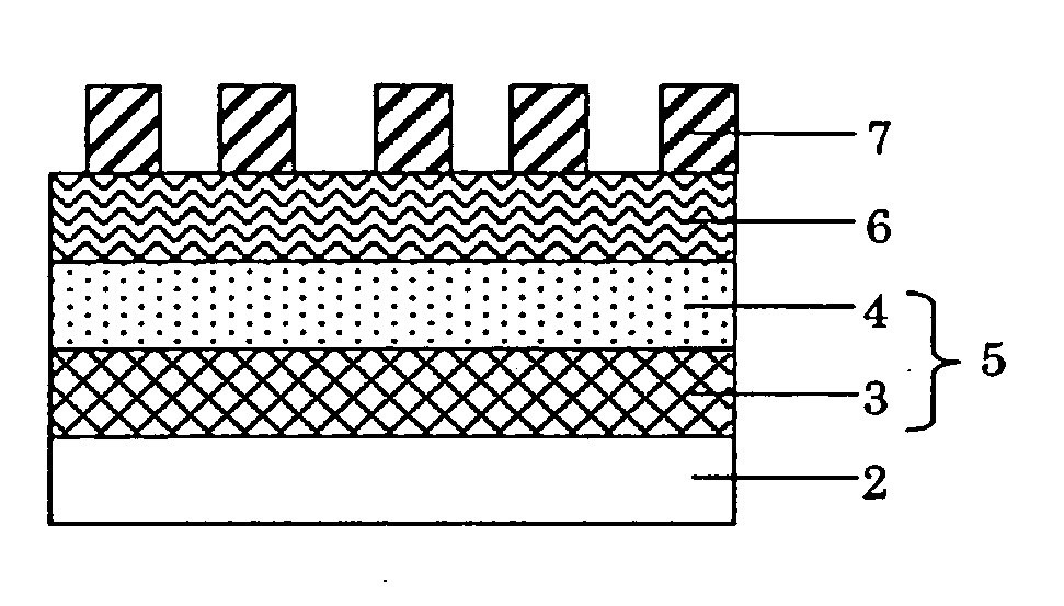
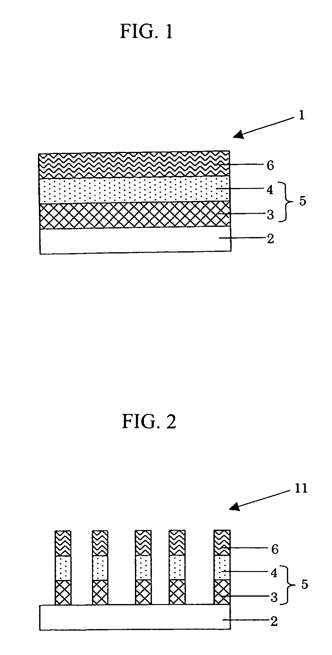
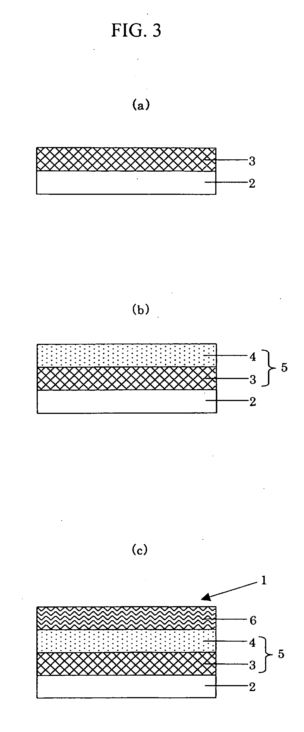
[0043] As shown in FIG. 1, in a photomask blank 1 according to Embodiment 1, a quartz glass substrate having both main surfaces and end surfaces subjected to precision polishing and a size of 6 inches×6 inches×0.25 inch is used as a translucent substrate 2.

[0044] On the translucent substrate 2, a Cr film of 500 angstrom is formed as a light-shielding film 3, a CrO (which means that chrome and oxygen are contained but does not specify content rates of these materials, and this is also applied to the following) film of 180 angstrom is formed as a reflection factor reducing film 4 and an MoSiON film of 100 angstrom is formed as an antireflective film 6.

[0045]FIG. 2 is a cross-sectional view showing a photomask according to Embodiment 1. This photomask 11 is formed by sequentially patterning the antireflective film 6, the reflection factor reducing film 4 and the light-shielding film 3 from an upper layer portion of the photomask blank 1.

[0046] A manufacturing method of the photomask...

embodiment 2

[0058] First, a translucent substrate 2 having a size of 6 inches×6 inches×0.25 inch obtained by subjecting main surfaces and end surfaces (side surfaces) of a quartz substrate to precision polishing was used, and a CrC film as a light-shielding film (layer) 3 was formed by reactive sputtering of an inline type sputtering apparatus using a Cr target in a mixed gas atmosphere of Ar and CH4 (Ar: 96.5 volume %, CH4: 3.5 volume %, and a pressure: 0.3 [Pa]).

[0059] Then, a CrON film as a reflection factor reducing film (layer) 4 was formed on the light-shielding film (layer) by reactive sputtering of the same inline type sputtering apparatus using a Cr target in a mixed gas atmosphere of Ar and NO (Ar: 87.5 volume %, NO: 12.5 volume %, a pressure: 0.3 [Pa]). Here, formation of the CrON film was carried out continuously with formation of the CrC film, and a total film thickness of the CrON film and the CrC film was 800 angstrom. This corresponds to a case where a boundary between the ligh...

embodiment 3

[0063] First, a quartz glass substrate having both main surfaces and end portions subjected to precision polishing and a size of 6 inches×6 inches×0.25 inch is used as a translucent substrate 2, then a CrC film (layer) as a light-shielding film 3 and a CrON film as a reflection factor reducing film (layer) 4 are continuously formed, and these steps are the same as those in Embodiment 2.

[0064] Subsequently, an MoSiON film having a film thickness of 100 angstrom was formed as an antireflective film 6 by reactive sputtering of a sheet type sputtering apparatus using an MoSi (Mo: 10 atom %, and Si: 90 atom %) target in a mixed gas atmosphere of Ar, N2 and O2 (Ar: 25 volume %, N2: 65 volume %, O2: 10 volume %, and a pressure: 0.13 [Pa]). Thereafter, scrub cleansing was performed to obtain a photomask blank 1.

[0065] Here, a transmission factor of the 100-angstrom MoSiON film used as the antireflective film was 91.7% in 248 nm and 86.7% in 193 nm like Embodiment 1 (however, a transmissio...


PUM

PropertyMeasurementUnit
wavelengthaaaaaaaaaa

Abstract

A low reflective photomask blank suitable for shortened exposure wavelengths is disclosed. A photomask blank (1) having a single-layer or multilayer light-shielding film (3) arranged on a translucent substrate (2) and mainly containing a metal is characterized by comprising an antireflective film (6), which at least contains silicon and oxygen and / or nitrogen, on the light-shielding film (3).

Description

TECHNICAL FIELD [0001] The present invention relates to a photomask used in manufacture of a semiconductor integrated circuit, a liquid crystal display apparatus or the like, a photomask blank which is an original plate of the photomask, and a pattern transfer method using the photomask. BACKGROUND ART [0002] In manufacture of a semiconductor integrated circuit, a liquid crystal display apparatus or the like, a photolithography method using a photomask is utilized in a microfabrication process. As this photomask, one having a light-shielding film pattern on a translucent substrate forms a general configuration of a photomask called a binary mask. Further, in recent years, in order to realize highly accurate pattern exposure, there is a photomask called a phase shift mask. As the phase shift mask, there is known a currently practically utilized halftone type phase shift mask which has a semi-translucent phase shift film pattern on a translucent substrate and has a light-shielding fil...

Claims


Application Information

Patent Timeline
Patent Type & Authority Applications(United States)
IPC IPC(8): G03F1/00C23C14/06G03F1/32G03F1/68G03F7/20H01L21/027
CPCG03F1/14G03F1/58G03F1/54G03F1/46G03F1/50G03F1/24G03F7/091H01L21/0276G03F1/62
Inventor KUREISHI, MITSUHIROMITSUI, HIDEOKI
Owner HOYA CORP
Why Eureka
Try Eureka