

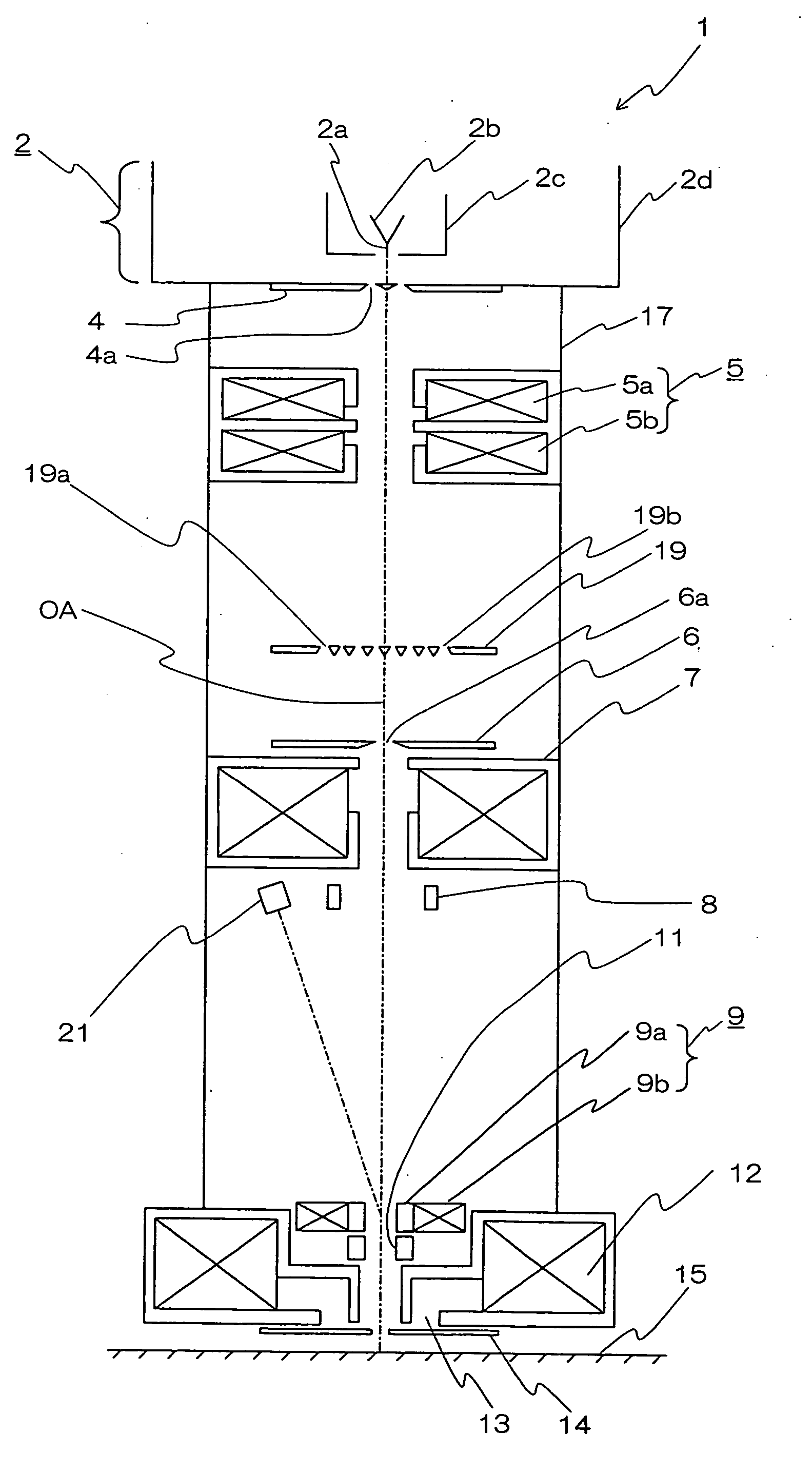
System and method for evaluation using electron beam and manufacture of devices
a technology of electron beam and electron beam, which is applied in the field of electron beam apparatuses, can solve the problems of inability to evaluate and/or form patterns, damage to cathodes, and inability to improve throughput in pattern evaluation and/or pattern formation, etc., and achieves short focal length, reduced space charge effect, and high current
- Summary
- Abstract
- Description
- Claims
- Application Information
AI Technical Summary
Benefits of technology
Problems solved by technology
Method used
Image

Examples
example 1
[0112] Sixteen beams with an electron gun comprising the LaB6 cathode, [0113] X-directional field size: 0.05 mm, [0114] Scanning return time: 5 μseconds, [0115] Registration time: 10 seconds, [0116] Sample loading / unloading time: 20 seconds, and [0117] Clock frequency: 100 MHz.
[0118] (1) Scanning time: [0119] [140×100 / (0.05×10⁻³)2]×10×10−9 sec×[1 / 16]=350 seconds
[0120] (2) Scanning flyback time: [0121] (140 / 0.05)×[100 / (16×5×10−5)]×5×10⁻⁶sec=175 seconds
[0122] (3) Stage flyback time: [0123] (140 / 0.05)×0.5 sec=140 seconds
[0124] (4) Registration+loading / unloading time=30 seconds [0125] Total: 695 seconds 12 minutes [0126] Throughput: 5 masks / hour
example 2
[0127] Scanning with four beams at 500 MHz with an electron gun comprising the TaC cathode, with the other conditions remaining unchanged from the above Example 1.
[0128] (1) Scanning time: [0129] [140×100 / (0.05×10⁻³)2]×2×10−9 sec×[1 / 4]=280 seconds
[0130] (2) Scanning flyback time: [0131] (140 / 0.5)×[100 / (4×5×10−5)]×5×10⁻⁶ sec=700 seconds
[0132] (3) Stage flyback time:=140 seconds
[0133] (4) Registration+loading / unloading time=30 seconds [0134] Total: 1150 seconds=19 minutes [0135] Throughput: 3.2 masks / hour
[0136] Turning now to flow charts in FIGS. 12 and 13, a method for manufacturing a semiconductor device by using the electron beam apparatus of the present invention will be described. The electron beam apparatus of the present invention is intended to provide evaluation of wafers during processing or after being processed in the flow charts shown in FIGS. 12 and 13.
[0137] As shown in FIG. 12, the method for manufacturing a semiconductor device, if divided schematically, include...
PUM
 Abstract
Description
Claims
Application Information