Metallized substrate

a technology of metal and substrate, applied in the direction of manufacturing tools, coatings, transportation and packaging, etc., can solve the problems of warping of substrate, coefficient of thermal expansion of metal and ceramic, and the inability to mount workpieces such as semiconductors in close contact with the substrate, etc., to achieve a thin, smooth surface, and little warping

Inactive Publication Date: 2006-03-23
SUMITOMO ELECTRIC IND LTD
View PDF5 Cites 26 Cited by
  • Summary
  • Abstract
  • Description
  • Claims
  • Application Information

AI Technical Summary

Benefits of technology

[0007] The present invention was designed in order to solve above described problems. Specifically, an object of the present invention is to provide a metallized substrate that has little warping, and has a dense, smooth surface.

Problems solved by technology

However, when the paste of a metal powder is baked onto the ceramic substrate, there is a problem in that the substrate becomes warped due to contraction in the volume of the metal powder from baking, and the difference in the coefficients of thermal expansions of the metal and the ceramic.
If the substrate becomes warped, a workpiece such as a semiconductor, for example, cannot be mounted in close contact with the substrate.
If a workpiece cannot be mounted in close contact with the substrate, where the substrate is to be used as a wafer prober, for example, there is a problem in that the workpiece cannot be adequately fixed in place by suction.
Furthermore, even if the workpiece is successfully fixed in place by suction, when a probe card is pressed against the workpiece, there are sections in the workpiece with which the probe pin cannot come into contact, or the workpiece is damaged.
Also, a plating film cannot be formed in large pores easily, and therefore pinholes tend to be formed.
Furthermore, there is also a problem that the thickness of the metal layer cannot be increased with a metal paste or plating or the like.

Method used


Image

  • Metallized substrate
  • Metallized substrate
  • Metallized substrate

Examples


embodiment 1

[0064] Substrates of aluminum nitride (AlN), silicon nitride (Si3N4), silicon carbide (SiC), alumina (Al2O3), a composite of aluminum and silicon carbide (Al—SiC), and a composite of silicon and silicon carbide (Si—SiC) were provided, each with a diameter of 330 mm and a thickness of 5 mm. The amount of warping in each of these substrates was 10 μm or less. A conductive film with a diameter of 310 mm and a thickness of 50 μm was formed in the middle of one side of these substrates by the wire flame spraying of aluminum (Al), nickel (Ni), copper (Cu), and stainless steel (SUS), and then an increase in the warping of the surface of the conductive film (in units of μm) was measured.

[0065] For the sake of comparison, a silver paste was prepared by mixing together 90 wt % of silver powder, 5 wt % of platinum powder, 2 wt % of ZnO2 powder, 2 wt % of B2O3 powder, and 1 wt % of SiO2 powder, and adding an organic solvent and a binder. A coating of this silver paste (Ag) was applied by scree...

embodiment 2

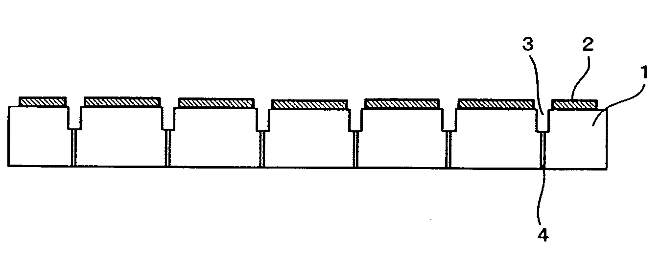
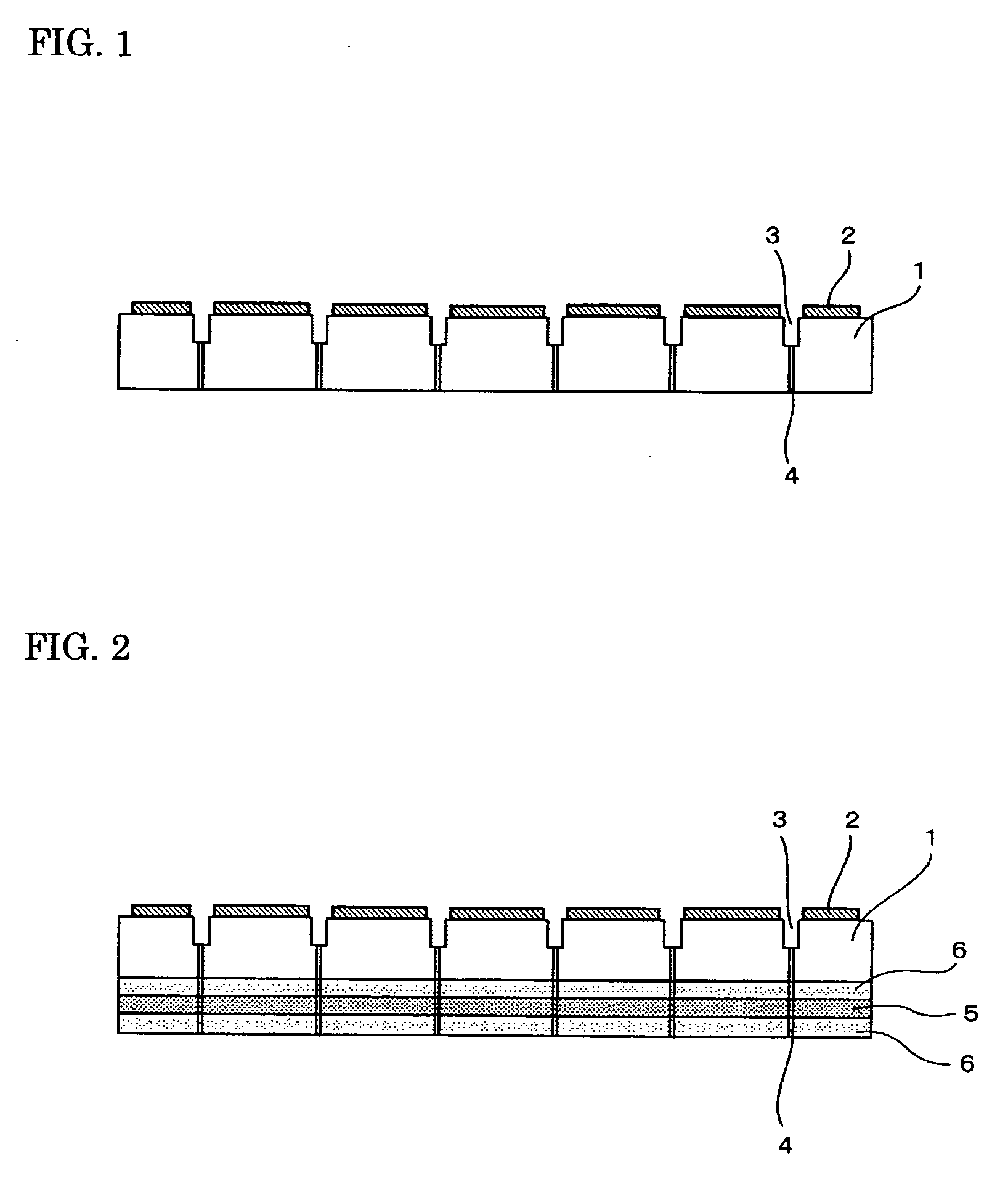
[0067] The substrates of Embodiment 1 having sprayed aluminum were provided. As shown in FIG. 1, three circular grooves 3 with respective diameters of 250 mm, 150 mm, and 50 mm were formed 2 mm wide and 2 mm deep by mechanical processing on the surface of an aluminum conductive film 2 formed on a substrate 1. Through-holes 4 were formed in these circular grooves. Four through-holes were formed in the groove with the diameter of 250 mm, three were formed in the groove with the diameter of 150 mm, and two were formed in the groove with the diameter of 50 mm to allow vacuum suction from the opposite side.

[0068] The surface of the conductive film was polished to varying degrees of surface roughness (Ra), and the suction properties of the wafer were examined. The results are shown in Table 2. In evaluating the suction properties, the sign ⊚ indicates that the suction property was very good and that sufficiently close contact was maintained even one minute after the completion of the vac...

embodiment 3

[0070] Twenty μm of nickel plating was applied on the conductive films of the metallized substrates used in Embodiment 2, and the surfaces of the nickel plating layers were polished to achieve the surface roughness values (Ra) shown in Table 3. The wafer suction properties were then examined, as in Embodiment 2. The results are shown in Table 3. The symbols are similar to those in Table 2.

TABLE 3SubstrateRaSuctionRaSuctionRaSuctionMaterial(μm)property(μm)property(μm)propertyAlN0.13⊚0.84◯1.49XSi3N40.18⊚0.91◯1.68XSiC0.17⊚1.0◯1.88XAl2O30.20⊚0.90◯1.47XAl—SiC0.13⊚0.78◯1.71XSi—SiC0.18⊚0.64◯1.79X

[0071] As can be seen from Table 3, even when plating is applied to the conductive film, the wafer can be adequately suctioned if the surface roughness Ra of the plating is 1.0 μm or less, and an even more preferable suctioning condition can be achieved if Ra is 0.2 μm or less.


PUM

PropertyMeasurementUnit
surface roughnessaaaaaaaaaa
surface roughness Raaaaaaaaaaa
surface roughnessaaaaaaaaaa

Abstract

The present invention provides a metallized substrate that has little warping and a fine, smooth surface. In the metallized substrate of the present invention, a conductive film is formed by spraying on the surface of a ceramic substrate or a composite substrate of a ceramic and a metal. The surface roughness of the conductive film formed by the spraying is preferably Ra≦1.0 μm. The surface of the conductive film may be a machined surface. The spraying is preferably arc spraying, plasma spraying, or flame spraying.

Description

TECHNICAL FIELD [0001] The present invention relates to a metallized substrate wherein a conductive film is formed on the surface of a ceramic substrate or a composite substrate of a ceramic and a metal, and the surface is made fine and smooth. The present invention further relates to a heating device that uses this metallized substrate and that is used in semiconductor manufacturing devices or semiconductor testing devices. The present invention still further relates to wafer probers, handlers, and testers and the like on which such heating device is mounted. BACKGROUND ART [0002] In the prior art, a heat treatment is conducted on a semiconductor substrate (wafer) as a workpiece during a testing step for a semiconductor. In other words, the wafer is heated to a higher temperature than the usual usage temperature, so that any semiconductor chips which have the possibility of failing are made to fail at an accelerated rate and are removed. This is a burn-in step, which is conducted t...

Claims


Application Information

Patent Timeline
Patent Type & Authority Applications(United States)
IPC IPC(8): C25D1/08B21D39/00B32B15/04C03C27/02
CPCC03C17/09C03C2217/77C23C4/06C23C4/12H05K1/0306H05K3/14Y10T428/12576H01L2924/0002H05K2203/1344Y10T428/12535Y10T428/12361Y10T428/12611H01L2924/00
Inventor NATSUHARA, MASUHIRONAKATA, HIROHIKOOTSUJI, FUMIO
Owner SUMITOMO ELECTRIC IND LTD
Why Eureka
Try Eureka