Method for manufacturing nitride semiconductor self-supporting substrate and nitride semiconductor self-supporting substrate

a technology of nitride semiconductor and self-supporting substrate, which is applied in the direction of polycrystalline material growth, crystal growth process, chemically reactive gas, etc., can solve the problems of cracks or breakage, difficult bulk crystal growth of nitride semiconductor, and inability to grow single crystal film, etc., to achieve excellent crystal quality, good productivity, and small warp

Active Publication Date: 2015-09-08
SHIN-ETSU HANDOTAI CO LTD
View PDF32 Cites 0 Cited by
  • Summary
  • Abstract
  • Description
  • Claims
  • Application Information

AI Technical Summary

Benefits of technology

[0014]In view of the above-explained problems, it is a main object of the present invention to provide a method for manufacturing a nitride semiconductor self-supporting substrate having an excellent crystal quality, small warp, and a large diameter with good productivity at a low cost.

Problems solved by technology

However, bulk crystal growth of a nitride semiconductor is difficult, and a GaN self-supporting substrate is just utilized for, e.g., a laser diode application having no problem in cost in a limited way.
In this case, since the sapphire substrate has a lattice constant different from that of GaN, a single-crystal film cannot be grown when GaN is directly epitaxially grown on the sapphire substrate.
However, even in growth of GaN using this buffer layer grown at a low temperature, the substrate after the epitaxial growth warps due to a difference in thermal expansion coefficient between the sapphire substrate and GaN, resulting in a problem of cracks or breakage.
Furthermore, warpage of the substrate after the epitaxial growth makes an exposure state of a fine pattern in photolithography uneven, thereby leading to a serious problem.
However, there still remains a problem that an inner strain of the GaN epitaxial layer due to a difference in thermal expansion coefficient between sapphire and GaN is locally relieved when the sapphire substrate is removed, and warp of the GaN substrate is thereby increased, thus breaking the substrate.
2, No. 3A, L217-219), but this method has a disadvantage that the substrate is apt to be cracked during a delamination process, thereby leading to a problem that a complicated processing is required to obtain a large GaN substrate with excellent reproducibility.
Therefore, a buffer layer is required, and a practical application of a GaN substrate having excellent crystallinity still has a problem because of a difference in growth temperature or melting point of the substrate.
Furthermore, there is also a problem that the GaN self-supporting substrate greatly warps.
However, according to this method, stably obtaining the GaN self-supporting substrate having a high crystal quality is difficult.

Method used


Image

  • Method for manufacturing nitride semiconductor self-supporting substrate and nitride semiconductor self-supporting substrate
  • Method for manufacturing nitride semiconductor self-supporting substrate and nitride semiconductor self-supporting substrate
  • Method for manufacturing nitride semiconductor self-supporting substrate and nitride semiconductor self-supporting substrate

Examples


example 1

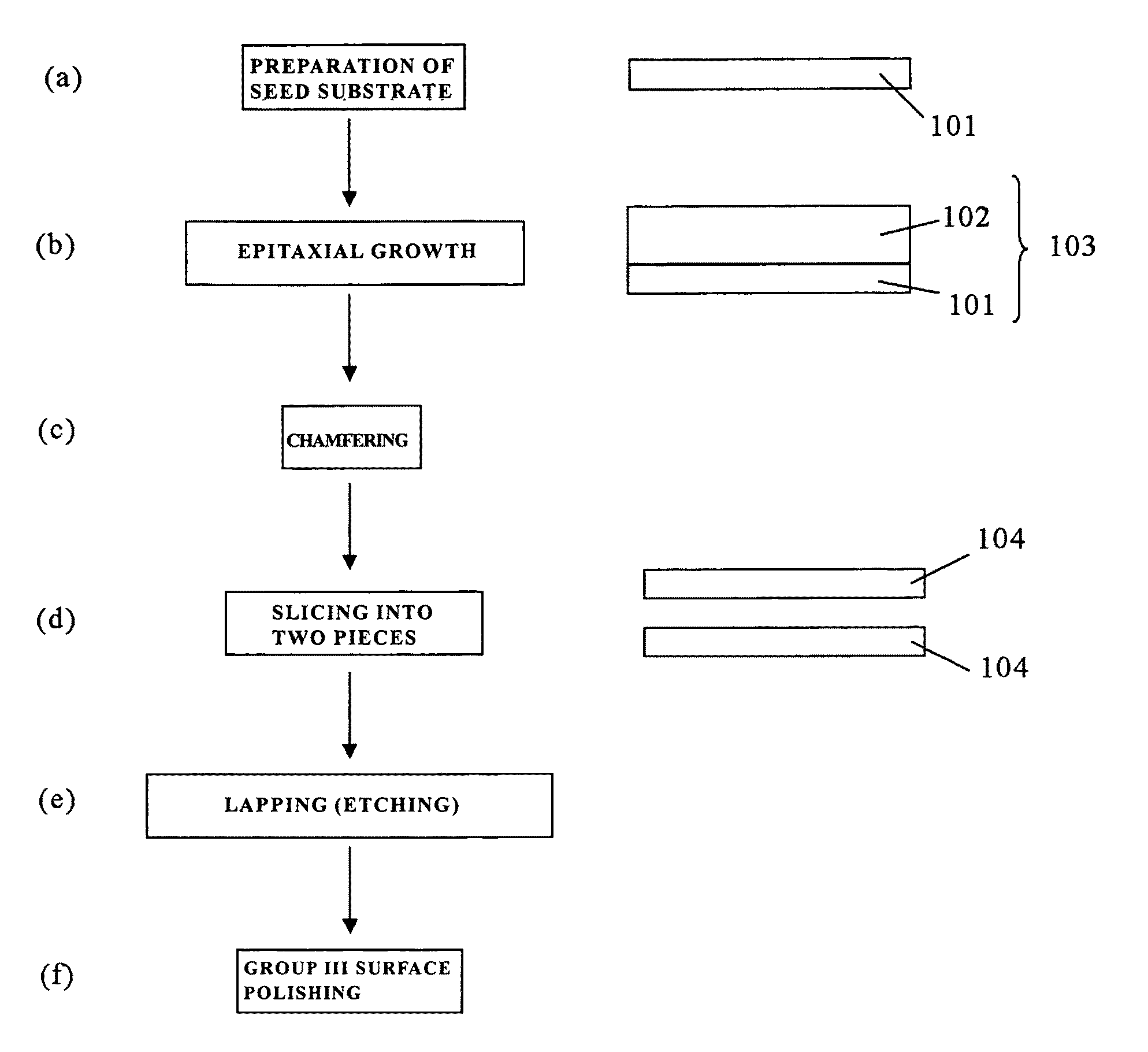
[0105]A GaN self-supporting substrate was manufactured as follows based on the method depicted in FIG. 1.

[0106]As seed substrates 101, eight GaN self-supporting substrates having a diameter of 50.8 mm (2 inches), a thickness of 400 μm, and a dislocation density of 1×10⁷ / cm2 or below were prepared (Step a), the dislocation density being obtained when a (0001) gallium surface is polished to have an epitaxial growth quality.

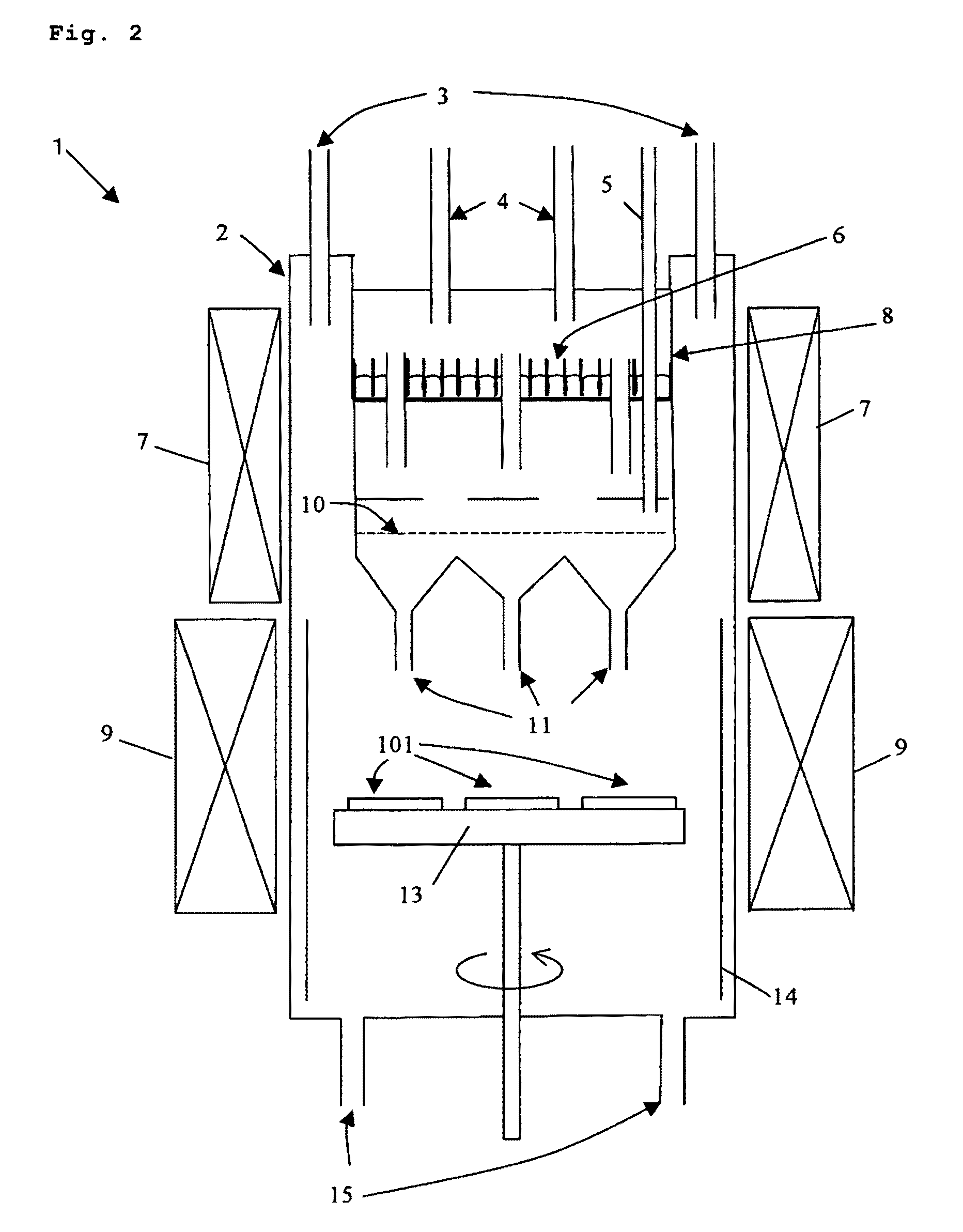
[0107]Then, such an epitaxial growth apparatus 1 as depicted in FIG. 2 was used to perform epitaxial growth of GaN as follows (Step b).

[0108]In a vertical chamber (a reaction tube made of quartz) 2 having an internal diameter of 200 mm, the eight seed substrates were mounted on a susceptor 13 with each (0001) gallium surface facing an upper side (Step a). Further, a gallium chloride generation tube 8 having 400 g of metal gallium put in a boat for gallium source 6 having partitions provided thereon at intervals of 1 cm was provided. The gallium chloride generation t...

example 2

[0120]Eight in the 16 GaN self-supporting substrates obtained in Example 1 were again used as seed substrates 101 to manufacture GaN self-supporting substrates as follows.

[0121]Each of the eight seed substrates 101 was a GaN self-supporting substrate having a diameter of 50.8 mm, a thickness of approximately 400 μm, a warp value of 25 μm or below, and a threading dislocation density of 5×10⁷ / cm2 or below as explained above (Step a).

[0122]Then, an HPVE apparatus 1 was used like Example 1 to perform growth wherein a growth time was set to 7 hours and 30 minutes (Step b). A thickness of an epitaxial layer 102 was 610 μm.

[0123]Subsequently, a chamfering step (Step c) was carried out with respect to an epitaxially grown substrate 103 like Example 1.

[0124]Then, a back-plate 35 was attached to an orientation flat portion with respect to the chamfered epitaxially grown substrate 103, and this substrate was set on a wafer stage 32 of such a wire saw as depicted in FIG. 5. Positional setting ...

example 3

[0127]Like Example 1, steps where epitaxial layers were simultaneously grown to 1 mm (=1000 μm) on three seed substrates 101 each having a threading dislocation density of 1×10⁷ / cm2 and epitaxially grown substrates 103 were thereby fabricated were carried out from the beginning. The three epitaxially grown substrates 103 were obliquely polished and etched with a solution of potassium hydroxide at a high temperature, and a distribution of a density of etch pits (dislocation pits) in a depth direction was checked. FIG. 9 is a graph showing a relationship between an epitaxial layer thickness and an etch pit density. An epitaxial layer thickness of 0 μm represents an interface between the epitaxial layer and the seed substrate 101 side. The dislocation density was increased beyond a dislocation density of the substrate in single digit or more on the initial stage of epitaxial growth, but it was gradually reduced toward the epitaxial surface to consequently approximate the dislocation de...


PUM

PropertyMeasurementUnit
thicknessaaaaaaaaaa
thicknessaaaaaaaaaa
thicknessaaaaaaaaaa

Abstract

The present invention provides a method for manufacturing a nitride semiconductor self-supporting substrate and a nitride semiconductor self-supporting substrate manufactured by this manufacturing method, the method including at least: a step of preparing a nitride semiconductor self-supporting substrate serving as a seed substrate; a step of epitaxially growing the same type of nitride semiconductor as the seed substrate on the seed substrate; and a step of slicing an epitaxially grown substrate subjected to the epitaxial growth into two pieces in parallel to an epitaxial growth surface. As a result, there is provided a method for manufacturing a large-diameter nitride semiconductor self-supporting substrate having an excellent crystal quality and small warp with good productivity at a low cost, etc.

Description

TECHNICAL FIELD[0001]The present invention relates to a self-supporting substrate of group III nitride semiconductor, GaN etc., and a manufacturing method thereof.BACKGROUND ART[0002]A group III nitride based compound semiconductor (a gallium nitride (GaN), an indium gallium nitride (InGaN), or a gallium aluminum nitride (GaAlN), etc.: which will be also simply referred to as a nitride semiconductor hereinafter) has recently started playing an important role as a material for a blue or ultraviolet light emitting diode (LED) or a laser diode (LD). Further, since a nitride semiconductor is superior in heat resistance or environment resistance or in high-frequency characteristics besides optical devices, electronic devices exploiting such characteristics have been positively developed.[0003]However, bulk crystal growth of a nitride semiconductor is difficult, and a GaN self-supporting substrate is just utilized for, e.g., a laser diode application having no problem in cost in a limited...

Claims


Application Information

Patent Timeline
Patent Type & Authority Patents(United States)
IPC IPC(8): C30B29/40C23C16/448C30B25/02H01L21/02H01L33/32
CPCC30B29/406C23C16/4488C30B25/02C30B29/403H01L21/02005H01L21/02008H01L21/0254H01L21/0262C23C16/01H01L21/302H01L33/02H01L21/20C23C16/34H01L21/67207
Inventor TAKAMIZAWA, SHOICHIWATANABE, MASATAKA
Owner SHIN-ETSU HANDOTAI CO LTD
Why Eureka
Try Eureka