Semiconductor device and method for fabricating the same

a technology of semiconductor devices and indium ions, applied in the direction of semiconductor devices, electrical equipment, transistors, etc., can solve the problems of abnormal diffusion of indium, low activation rate of indium ions, and inability to obtain sufficient activation concentration, so as to reduce the size of the device, suppress the transient enhanced diffusion of a dopant, and increase the activation rate of the introduced dopant

Inactive Publication Date: 2006-03-30
PANASONIC CORP
View PDF11 Cites 37 Cited by
  • Summary
  • Abstract
  • Description
  • Claims
  • Application Information

AI Technical Summary

Benefits of technology

[0026] In the second inventive semiconductor device, the carbon added to the pocket doped layers formed below the sides of the gate electrode suppresses transient enhanced diffusion of a dopant in the pocket doped layers, while increasing the activation rate of the introduced dopant. Thus, steep dopant-concentration profiles having a shallow junction, which are necessary to reduce the device size, are realized in the pocket doped layers, while the sufficiently increased activation concentration in the pocket doped layers suppresses depletion in the channel doped layer, thereby making i

Problems solved by technology

However, in the conventional semiconductor-device fabrication method, if indium ions are used as a dopant for forming doped layers such as the P-type channel doped layer 103 or the P-type pocket doped layers 107, a problem occurs in that the activation rate of the indium ions is low and hence sufficient activation concentration cannot be obtained.
As a result, transient enhanced diffusion (hereinafter simply referred to as “TED”) occurs, which also produces a problem in that abnormal diffusion of the indium is caused during the TED.
In many cases, those excess point defects

Method used


Image

  • Semiconductor device and method for fabricating the same
  • Semiconductor device and method for fabricating the same
  • Semiconductor device and method for fabricating the same

Examples


first embodiment

[0061] A first embodiment of the present invention will be described with reference to the accompanying drawings.

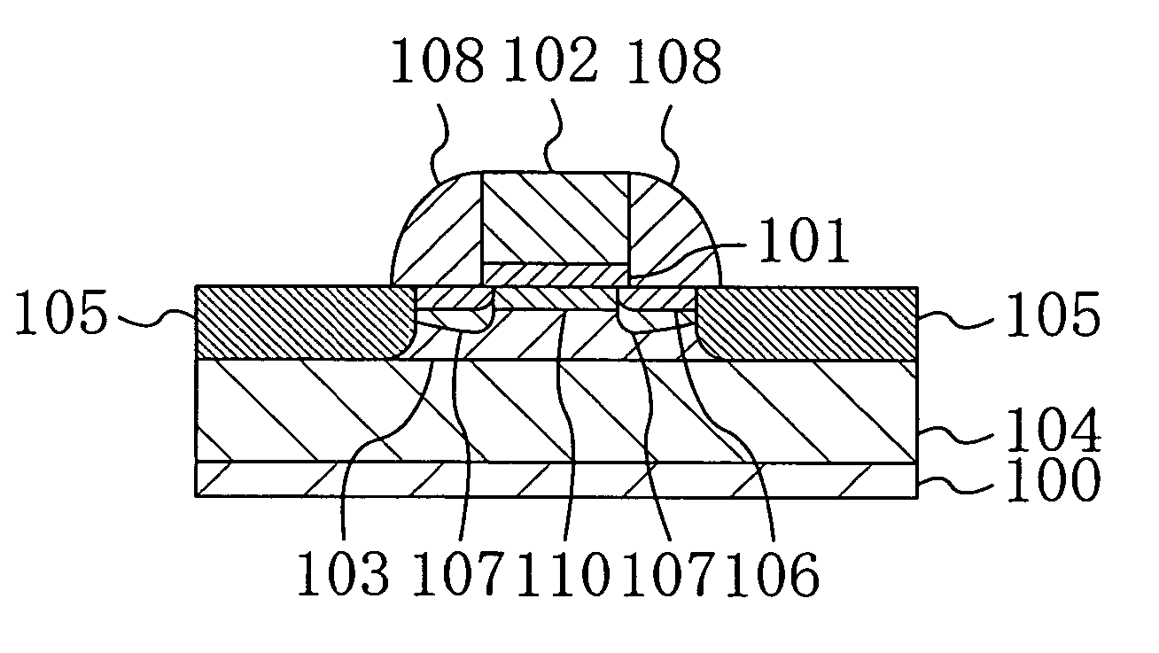
[0062]FIG. 1 illustrates a cross-sectional structure of a semiconductor device, a MIS transistor, according to the first embodiment of the present invention. As shown in FIG. 1, the MIS transistor of the first embodiment includes a gate insulating film 101 selectively formed on the principal surface of a semiconductor substrate 100 made of P-type silicon (Si), and a gate electrode 102 formed on the gate insulating film 101. The gate insulating film 101 is made of silicon dioxide (SiO2) and has a thickness of about 1.5 nm, while the gate electrode 102 is made of polysilicon or polymetal and has a thickness of about 150 nm.

[0063] Sidewalls 108 made of, e.g., silicon nitride (SiNx, for example, Si3N4) are formed on the semiconductor substrate 100 on both lateral faces of the gate insulating film 101 and gate electrode 102.

[0064] A P-type channel doped layer 103 is formed ...

second embodiment

[0080] Hereinafter, a second embodiment of the present invention will be described with reference to the accompanying figures.

[0081]FIG. 4 illustrates a cross sectional structure of a semiconductor device, a MIS transistor, according to the second embodiment of the present invention. In FIG. 4, the same members as those of FIG. 1 are identified by the same reference numerals and the description thereof will be omitted herein.

[0082] As shown in FIG. 4, in the MIS transistor of the second embodiment, a P-type channel doped layer 103, which is located in a semiconductor substrate 100 beneath a gate electrode 102, is formed spaced apart from the inner end portions of N-type heavily doped source / drain layers 105.

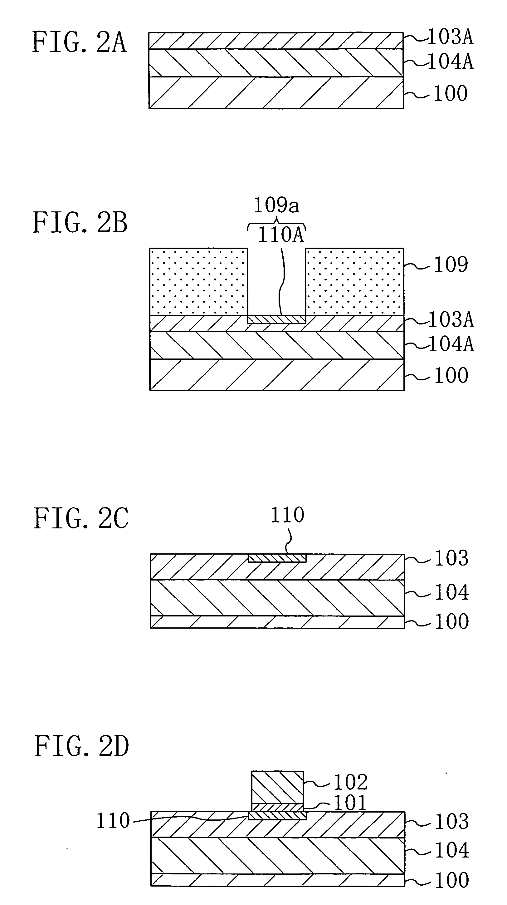
[0083] Hereinafter, with reference to the accompanying figures, it will be described how to fabricate a semiconductor device having the above structure.

[0084]FIGS. 5A through 5D and FIGS. 6A through 6D are cross-sectional views indicating process steps for fabricating a semic...

third embodiment

[0099] Hereinafter, a third embodiment of the present invention will be described with reference to the accompanying figures.

[0100]FIG. 7 illustrates a cross sectional structure of a semiconductor device, a MIS transistor, according to the third embodiment of the present invention. In FIG. 7, the same members as those of FIG. 1 are identified by the same reference numerals and the description thereof will be omitted herein.

[0101] As shown in FIG. 7, in the MIS transistor of the third embodiment, a gate electrode 115 is made of metal such as tungsten (W) or tantalum nitride (TaN) and a gate insulating film 114 is formed not only on the principal surface of a semiconductor substrate 100 but also between the gate electrode 115 and the inner lateral faces of sidewalls 108.

[0102] Hereinafter, with reference to the accompanying figures, it will be described how to fabricate a semiconductor device having the above structure.

[0103]FIGS. 8A through 8D and FIGS. 9A through 9E are cross-se...


PUM


Abstract

The semiconductor device of the present invention includes: a gate insulating film formed on a semiconductor region of a first conductivity type; a gate electrode formed on the gate insulating film; and a channel doped layer of the first conductivity type formed in the semiconductor region beneath the gate electrode. The channel doped layer contains carbon as an impurity.

Description

CROSS-REFERENCE TO RELATED APPLICATION [0001] This application is related to Japanese Patent Application No. 2004-279076 filed on Sep. 27, 2004, whose priority is claimed under 35 USC §119, the disclosure of which is incorporated herein by reference in its entirety. BACKGROUND OF THE INVENTION [0002] The present invention relates to semiconductor devices and methods for fabricating the devices, and more particularly relates to a MIS semiconductor device which can be reduced in size and has a doped layer having a shallow junction depth and a low resistance, and to a method for fabricating the semiconductor device. [0003] As the number of devices included in a semiconductor integrated circuit continues to increase, MIS transistors are required to be further reduced in size. To that end, MIS transistors need to have a channel doped layer having a shallow junction depth and a low resistance (see Japanese Laid-Open Publication No. 2002-33477, for example.) [0004] Hereinafter, with refere...

Claims


Application Information

Patent Timeline
IPC IPC(8): H01L21/336
CPCH01L21/2253H01L21/26506H01L29/105H01L29/7833H01L29/66545H01L29/6659H01L29/66492H01L21/2658H01L21/26513
Inventor NODA, TAIJI
Owner PANASONIC CORP
Why Eureka
Try Eureka