
Solid-state imaging device and method of manufacturing the same

a solid-state imaging and imaging device technology, applied in the field of solid-state imaging devices, can solve the problems of interconnection delay and difficulty in reducing dark current, and achieve the effect of effective reduction of dark curren

Inactive Publication Date: 2006-04-06
NEC ELECTRONICS CORP
View PDF5 Cites 6 Cited by
  • Summary
  • Abstract
  • Description
  • Claims
  • Application Information

AI Technical Summary

Benefits of technology

[0011] According to the present invention, since the titanium-containing film is selectively formed within the contact plug, adsorption of hydrogen under the metal interconnect can be suppressed, and consequently the dark current can be reduced. Moreover, since the titanium-containing film is formed within the contact plug, adherence between the contact plug and the electroconductive region can be improved. Therefore, the contact resistance between the contact plug and the electroconductive region can be reduced. Thus, the interconnect delay can be suppressed. In the present invention, the adhesive film may have a structure, for example, that covers the whole bottom and side surfaces of the contact plug. With this structure, the adherence between the contact plug and the electroconductive region can be improved more surely.
[0012] In the present invention, the titanium-containing film may be formed only in a lower part and on a side face of the contact plug. Moreover, the solid-state imaging device may have a structure where the insulating film and the metal interconnect are in direct contact with each other. With this structure, adsorption of hydrogen under the metal interconnect can be controlled even more surely.
[0020] According to the present invention, since the titanium-containing film is selectively formed within the contact plug, the dark current can be reduced effectively without increasing the contact resistance.

Problems solved by technology

However, when Ti metal or an alloy material containing Ti exists under the metal interconnect, these metal materials adsorb hydrogen, and hence it is difficult to reduce the dark current.
However, with the technologies disclosed in the above-mentioned Japanese Laid-open patent application No. 2003-229556 and Japanese Laid-open patent application No. 1996-37236, contact resistance between the contact plug and an electroconductive region in contact with an bottom surface of the contact plug increases to cause interconnect delay.

Method used


Image

  • Solid-state imaging device and method of manufacturing the same
  • Solid-state imaging device and method of manufacturing the same
  • Solid-state imaging device and method of manufacturing the same

Examples


first embodiment

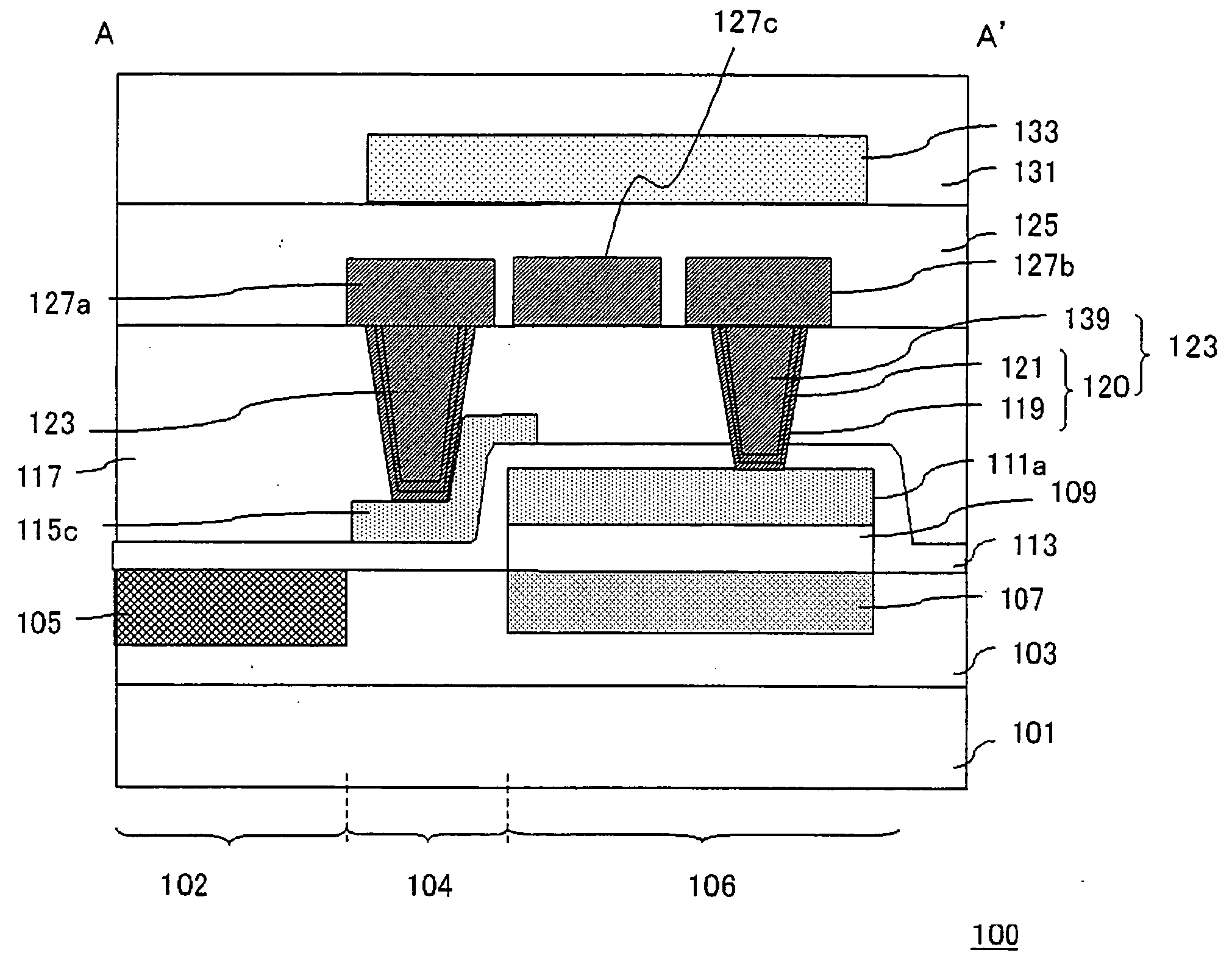
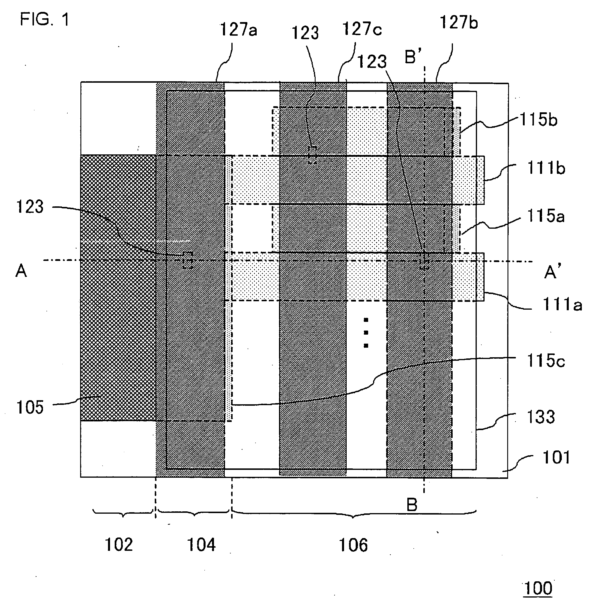
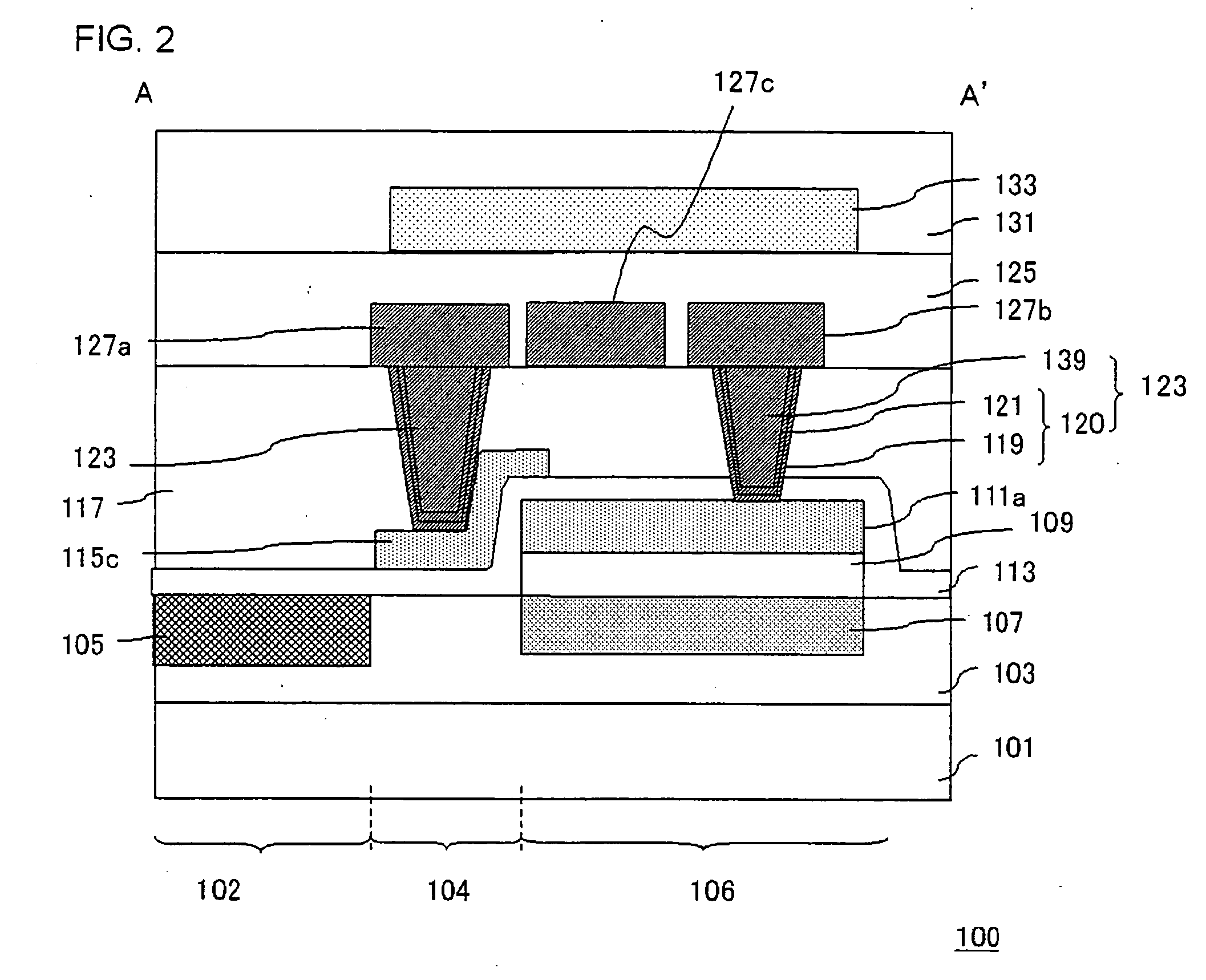
[0033]FIG. 1 is a plan view showing a structure of a solid-state imaging device according to this embodiment. A solid-state imaging device 100 shown in FIG. 1 is a one-dimensional CCD image sensor. FIG. 2 is an A-A′ cross-sectional view of the solid-state imaging device 100 in FIG. 1. FIG. 3 is a B-B′ cross-sectional view of the solid-state imaging device 100 in FIG. 1.

[0034] The solid-state imaging device 100 shown in FIGS. 1 to 3 comprises an N-type semiconductor substrate 101, electroconductive regions (a first polycrystalline silicon electrode 111a and a second polycrystalline silicon electrode 115c) provided on the N-type semiconductor substrate 101, an insulating film (a second insulating interlayer 117) formed on the electroconductive region, Al interconnects (first Al interconnects 127a, 127b) provided on the insulating film, contact plugs 123 each of which is provided in the insulating film and connects the lower surface of the Al interconnect and the electroconductive reg...

second embodiment

[0065]FIG. 7 is a cross-sectional view showing a structure of a solid-state imaging device according to this embodiment. FIG. 7 corresponds to a figure viewed from the same direction as that in FIG. 2. A solid-state imaging device 140 shown in FIG. 7 is a two-dimensional CCD image sensor that employs the basic structure shown in FIGS. 1 to 3.

[0066] Also in the solid-state imaging device 140 shown in FIG. 7, the adhesive film 120 is selectively formed within the contact plug 123 that connects the first polycrystalline silicon electrode 111 and the first Al interconnect 127 in a region between the first Al interconnect 127 and the first polycrystalline silicon electrode 111, and the adhesive film 120 is not formed in any region other than the region where the bottom surface of the first Al interconnect 127 is in contact with the contact plug 123. Therefore, the same effect as that of the solid-state imaging device 100 shown in FIGS. 1 to 3 can be achieved.

third embodiment

[0067] In the above embodiments, the cases where the solid-state imaging device was the CCD image sensor were illustrated. However, the structure of the present invention is also applicable to the CMOS (complementary metal oxide semiconductor) image sensor.

[0068]FIG. 8 is a cross-sectional view showing a structure of a CMOS image sensor of this embodiment. FIG. 8 corresponds to a view of the CMOS image sensor viewed from the same direction as that of FIG. 2. A solid-state imaging device 150 shown in FIG. 8 comprises a P-type semiconductor substrate 141, the photodiode 105 formed on the surface of the P-type semiconductor substrate 141, and an N+ well 145 that is formed on the surface of the P-type semiconductor 141 being placed side by side with the photodiode 105, and a LOCOS (local oxidation of silicon) isolating adjacent the N+ wells 145.

[0069] Moreover, the solid-state imaging device 150 has a gate insulating film (not shown in the drawings) formed on the N+ well 145 and the f...


PUM

PropertyMeasurementUnit
electroconductiveaaaaaaaaaa
charge transferaaaaaaaaaa
insulatingaaaaaaaaaa

Abstract

The invention reduces dark current of a solid-state imaging device. A solid-state imaging device containing photodiode comprises: a diffusion layer placed side by side with the photodiode on the surface of an N-type semiconductor substrate; a first polycrystalline silicon electrode provided on the diffusion layer; a first Al interconnect provided on the first polycrystalline silicon electrode; a contact plug connecting the lower surface of the first Al interconnect and the first polycrystalline silicon electrode; and an adhesive film that is a titanium-containing film selectively provided within the contact plug.

Description

[0001] This application is based on Japanese patent application NO. 2004-293981, the content of which is incorporated hereinto by reference. BACKGROUND OF THE INVENTION [0002] 1. Field of the Invention [0003] This invention relates to a solid-state imaging device and a method of manufacturing the same. [0004] 2. Description of the Related Art [0005] Conventionally, the solid-state imaging device of a CCD (charge coupled device) type or a CMOS type is a combination of photodiodes having a photoelectric conversion function and a transfer CCD transferring charges or a gate device formed on the surface of a semiconductor substrate with gate electrodes and a interconnect layer formed on these elements (Japanese Laid-open patent application No. 2003-229556). Japanese Laid-open patent application No. 2003-229556 discloses that metal Ti (titanium) or an alloy material containing Ti is used on and under the interconnect layer and in the vicinity of a plug layer of the solid-state imaging dev...

Claims


Application Information

Patent Timeline
Patent Type & Authority Applications(United States)
IPC IPC(8): H01L21/00H01L27/148H04N25/00
CPCH01L27/14636H01L27/14687H01L27/14843
Inventor UCHIYA, SATOSHIMORIYA, TAROYAMAMOTO, JUNICHI
Owner NEC ELECTRONICS CORP
Learn More