Heat treatment jig for semiconductor wafer

a heat treatment jig and semiconductor wafer technology, which is applied in the direction of charging supports, lighting and heating apparatus, furniture, etc., can solve the problems of deterioration of the planarity of the semiconductor wafer, increase of leakage current in the lsi device, and/or defect-laden products that are not usable, so as to improve the surface planarity due to the deflection of the heat treatment jig, and prevent the strain of surface machining

Active Publication Date: 2006-04-13
SUMCO CORP
View PDF10 Cites 9 Cited by
  • Summary
  • Abstract
  • Description
  • Claims
  • Application Information

AI Technical Summary

Benefits of technology

[0025] (a) By specifically controlling the thickness of a heat treatment jig, the surface planarity due to the deflection of the heat treatment jig is improved, and the bend of the heat treatment jig due to the tare stress and the strain in association with surface machining can be also prevented.
[0026] However, it should be noted that, when the heat treatment jig becomes thicker, the heat capacity thereof gets large, adversely affecting the heat-up/cool-down characteristic, and the number of semiconductor wafers to be charged decreases, thereby reducing the productivity

Problems solved by technology

With regard to a conventional heat treatment boat, said tare stress affects very much in case that the heat treatment is conducted for semiconductor wafers of 300 mm in diameter, thus resulting in making defects-laden products not to be usable.
Both thermal stress and tare stress as above are known to cause crystal defects called slips within semiconductor wafers during heat treatments.
The slips end up in an increase of a leakage current in LSI device and/or deterioration of planarity of semiconductor wafers.
Nonetheless, as the diameter of semiconductor wafers increases recently, the incurred tare stress tends to be increased notably, thereby aggravating an inhomogeneous distribution of tare stresses in case of a heat treatment boat shown in above FIG. 1 where a three- or four-point supporting system is applied at the peripheral region of the wafer backside, and thus resulting in generation of sli

Method used


Image

  • Heat treatment jig for semiconductor wafer
  • Heat treatment jig for semiconductor wafer
  • Heat treatment jig for semiconductor wafer

Examples


example 1

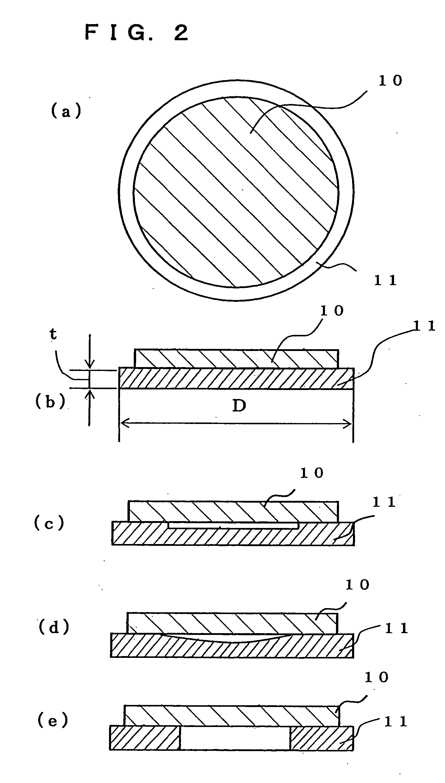
[0088] In Example 1, the heat treatment jig having a plurality of protruded portions formed as shown in above FIG. 6 is made. To that end, as shown in above FIG. 7, silicon is used for substrate member and the jig is processed to have a disk-type structure comprising 304 mm diameter, 2.5 mm thickness, 0.04 mm planarity in the concentric direction and 0.04 mm planarity in the diametrical direction (step (a)).

[0089] On the disk thus obtained, the masking treatment with circular protective seals 18 of 8.0 mm in diameter is carried out at every 1.0 mm pitch (step (b)), the blast treatment B is applied to scrape off the disk surface by an amount of 50 μm (step (c)), and then the circular protective seals 18 are ripped off to finally reveal protruded portions 15, 16, 17 (step (d)).

[0090] In addition, by applying a benign blast treatment onto the whole surface of the disk-type jig 11 thus obtained, the heat treatment jig with surface roughness (Ra value) of 1.5 μm is completed.

[0091] By...

example 2

[0092] In Example 2, SiC coating is applied. Silicon is used for the substrate material and the jig is processed to have a disk-type figuration comprising 304 mm diameter, 2.0 mm thickness, 0.02 mm planarity in the concentric direction and 0.06 mm in the diametrical direction. Next, by applying the blast treatment, the surface roughness (Ra value) of 2.5 μm is secured, SiC coating is subsequently applied for 20 μm deposition in conversion, and a light polishing is provided in succession in order to remove the region of abnormal growth by SiC, followed by the blast treatment to obtain the heat treatment jig with final surface roughness (Ra value) of 1.9 μm.

[0093] The heat treatment jig thus made is used for heat treatment under above condition and silicon wafers are observed for slip generation, whereby no slip is generated.

example 3

[0094] In Example 3, silicon carbide is used for the substrate material and the jig is processed to have a disk-type figuration comprising 304 mm diameter, 2.0 mm thickness, 0.08 mm planarity in the concentric direction and 0.19 mm in the diametrical direction, followed by the blast treatment for obtaining the surface roughness (Ra value) of 1.0 μm.

[0095] The heat treatment jig thus made is used for heat treatment under above condition and silicon wafers are observed for slip generation, whereby several slips of about 20-30 mm are generated.


PUM


Abstract

A heat treatment jig by the invention comprising: the diameter of a disk-type structure being 60% or more of that of loaded semiconductor wafers; the thickness being 1.0 mm or more but 10 mm or less; the surface roughness Ra of 0.1 μm or more but 100 μm or less at a contacting surface with the wafers; and the surface planarity being specifically controlled in the concentric direction as well as in the diametrical direction, otherwise in place of above planarity, comprising a controlled maximum height in such a way that the maximum height is obtained by the flatness measurement at the multiple positions and the difference between said maximum height and the hypothetical-average-height-plane thus set is 50 μm or less, can reduce the slip generation due to the close adhesion of the wafers and the jig. Owing to this, even if the wafers having large tare weight should be heat-treated, the slip generation can be effectively prevented, thus enabling the jig to be widely used as the reliable heat treatment jig for semiconductor substrates.

Description

CROSS-REFERENCE TO RELATED APPLICATIONS [0001] This application is a continuation-in-part of International Application No. PCT / JP2004 / 003442 filed Mar. 15, 2004. This PCT application was not in English as published under PCT Article 21(2).FIELD OF THE INVENTION [0002] The present invention relates to a heat treatment jig for use in a heat treatment boat of a vertical heat treatment furnace, more particularly, to a heat treatment jig for large diameter semiconductor wafers that can suppress the generation of slips as crystal defects during heat treatment at high temperature. BACKGROUND ART [0003] A semiconductor wafer that is processed in LSI device fabrication process is repeatedly subjected to a high temperature heat treatment in fabrication steps such as oxidation, diffusion and film deposition. In such a heat treatment, if an inhomogeneous temperature distribution should be generated within a wafer surface, the thermal stress is incurred thereby. [0004] Meanwhile, depending on th...

Claims


Application Information

Patent Timeline
IPC IPC(8): F27D5/00H01L21/00H01L21/673H01L21/687
CPCH01L21/67103H01L21/67306H01L21/68757H01L21/68735H01L21/6875H01L21/67309H01L21/324
Inventor ADACHI, NAOSHI
Owner SUMCO CORP
Why Eureka
Try Eureka