

Organic electronic device and method for producing the same
- Summary
- Abstract
- Description
- Claims
- Application Information
AI Technical Summary
Benefits of technology
Problems solved by technology
Method used
Image

Examples
example 1
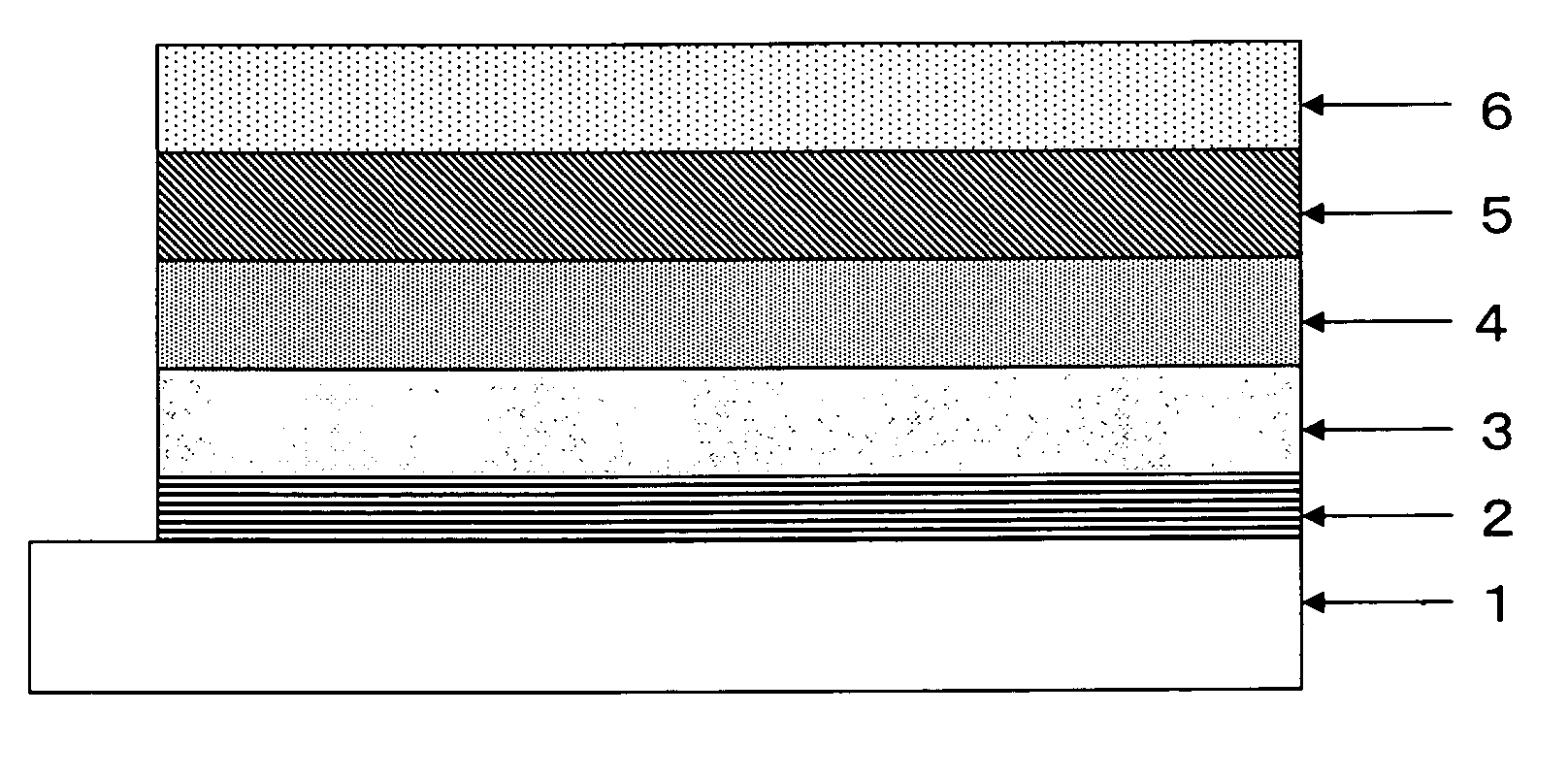
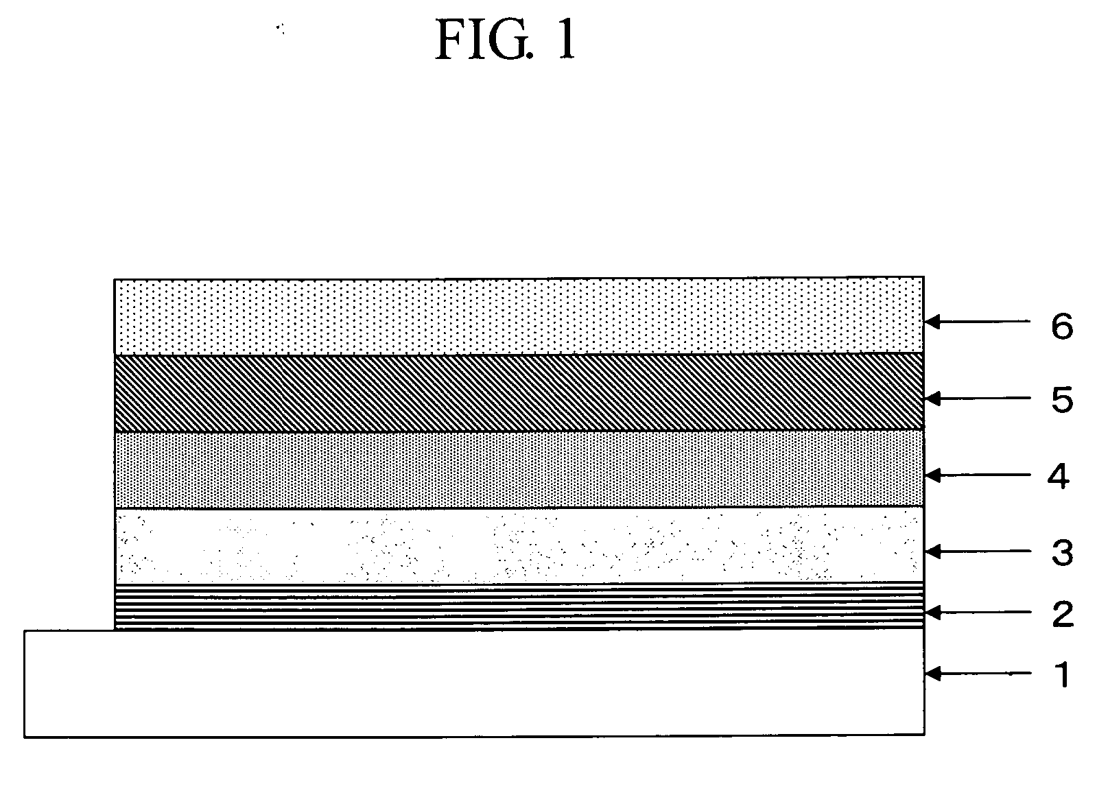
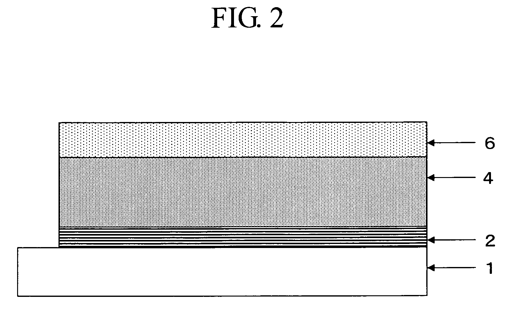
[0259] (Formation of Anode)
[0260] A transparent glass substrate (non-alkali glass NA 35; manufactured by NH Techno Glass Corporation) having a length to width dimension of 40 mm×40 mm and a thickness of 0.7 mm was prepared as a substrate. After washing the transparent glass substrate in accordance with the predetermined method, a thin film (thickness of 130 nm) of indium-zinc-oxide compound (IZO) was formed by a sputtering method. In forming the IZO thin film, a mixed gas of Ar and O2 (volume ratio of Ar:O2=100:1) was used as a sputtering gas, pressure was set as 0.1 Pa, and DC output was set as 150 W.
[0261] Next, a photosensitive resist (OFPR-800; manufactured by TOKYO OHKA KOGYO CO., LTD.) was applied on the anode followed by mask exposure, development (using NMD3 (developing solution); manufactured by TOKYO OHKA KOGYO CO., LTD.) and etching, thereby, the anode was formed in a pattern.
[0262] (Formation of Positive Hole Injection Transporting Layer)
[0263] Next, after washing th...
example 2
[0275] The process same as in Example 1 was carried out as far as the electron injection transporting layer was formed. Then, a cathode was formed using a metal comprising gallium:indium:tin (weight ratio of 50:25:25). That is, the alloy was melted by a heat treatment and coated to form the cathode in a predetermined pattern.
[0276] A current density upon impressing a voltage of 6 V on the organic EL element was about 100 mA / cm2. A luminance observed from the anode side was about 10,000 cd / m2. The results clearly show that a good element characteristic can be obtained even by forming the electron injection transporting layer comprising lithium diisopropylamide by coating, and then, forming the cathode by coating.
example 3
[0277] An organic EL element was produced similarly as Example 1 except that an electron injection transporting layer comprising lithium tetramethylcyclopentadiene was formed. A current density upon impressing a voltage of 6 V on the organic EL element was about 50 mA / cm2. A luminance observed from the anode side was about 5,000 cd / m2. The results clearly show that a good element characteristic can be obtained even by forming the electron injection transporting layer comprising lithium tetramethylcyclopentadiene by coating and using a metal having a large work function as the cathode.
PUM
| Property | Measurement | Unit |
|---|---|---|
| Structure | aaaaa | aaaaa |
| Electric charge | aaaaa | aaaaa |
| Electron affinity | aaaaa | aaaaa |
Abstract
Description
Claims
Application Information