GaN-based semiconductor integrated circuit

a semiconductor and integrated circuit technology, applied in the direction of semiconductor devices, diodes, electrical apparatuses, etc., to achieve the effect of reducing the energy loss in the junction region, reducing the amount of heat generated corresponding to the energy loss, and high withstanding voltag

Inactive Publication Date: 2006-04-20
FURUKAWA ELECTRIC CO LTD
View PDF4 Cites 45 Cited by
  • Summary
  • Abstract
  • Description
  • Claims
  • Application Information

AI Technical Summary

Benefits of technology

[0014] The Schottky diode included in the aforesaid GaN-based semiconductor integrated circuit has a composite anode consisting of a first anode and a second anode. Since the Schottky barrier formed between the first anode and the GaN-based semiconductor layer is lower than the Schottky barrier formed between the second anode and the GaN-based semiconductor layer, the on-state voltage required to give rise to a forward current when the Schottky diode is forward biased is a low voltage, depending only on the height of the Schottky barrier formed between the first anode and the GaN-based semiconductor layer. Consequently, the energy loss in the junction region reduces, and hence, the amount of heat generated corresponding to the energy loss can be kept small. Further, a reverse leak current produced when the Schott

Problems solved by technology

Using, in a power module, a semiconductor integrated circuit of a device structure shown in FIG. 10A including Si-based semiconductor devices has, however, the following problem: In the power modu

Method used


Image

  • GaN-based semiconductor integrated circuit
  • GaN-based semiconductor integrated circuit
  • GaN-based semiconductor integrated circuit

Examples


embodiment 1

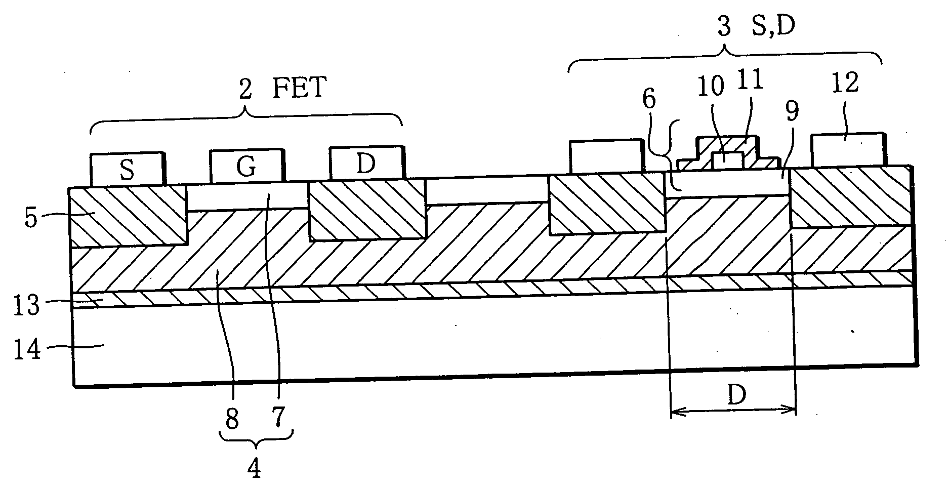
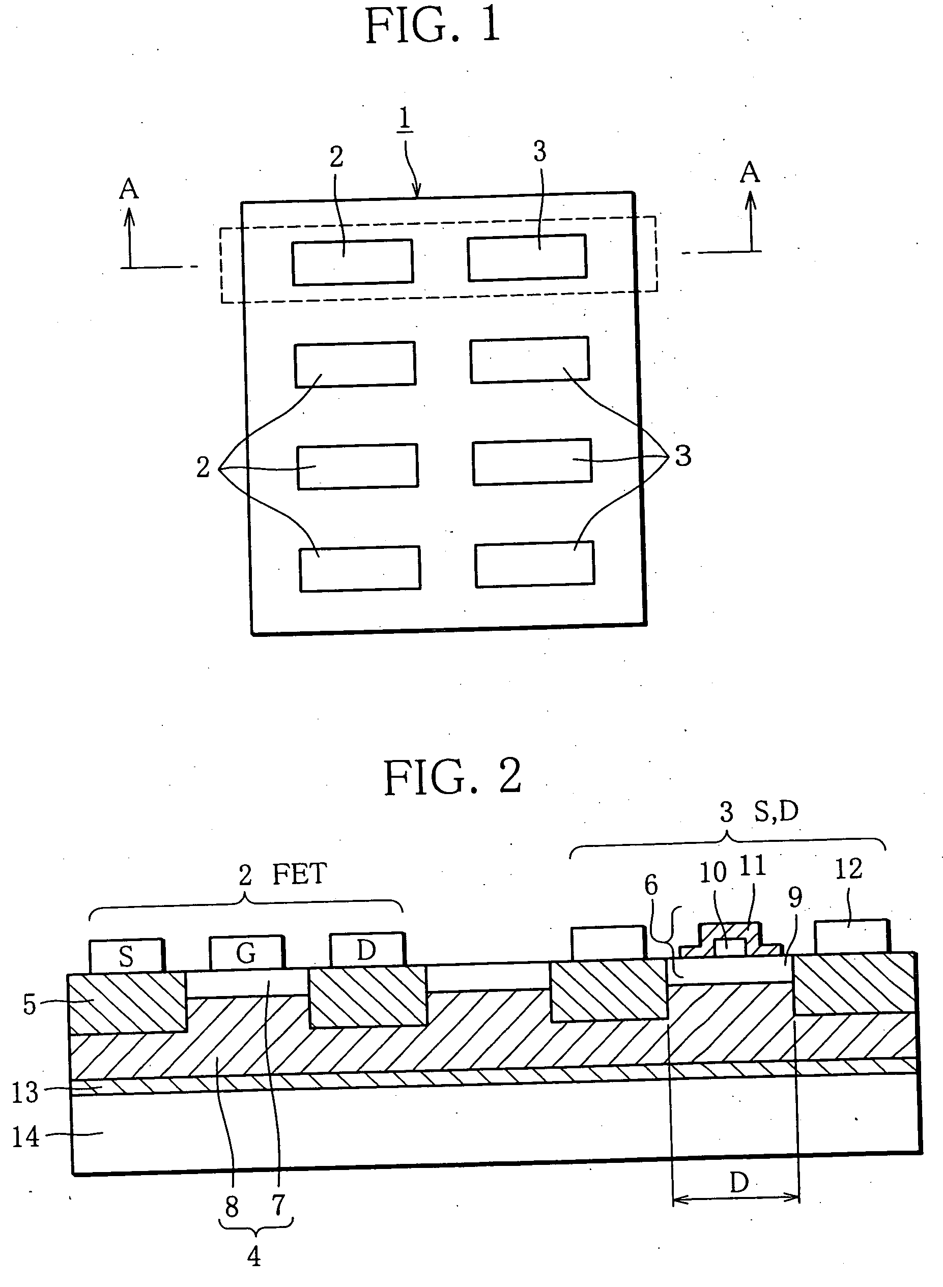
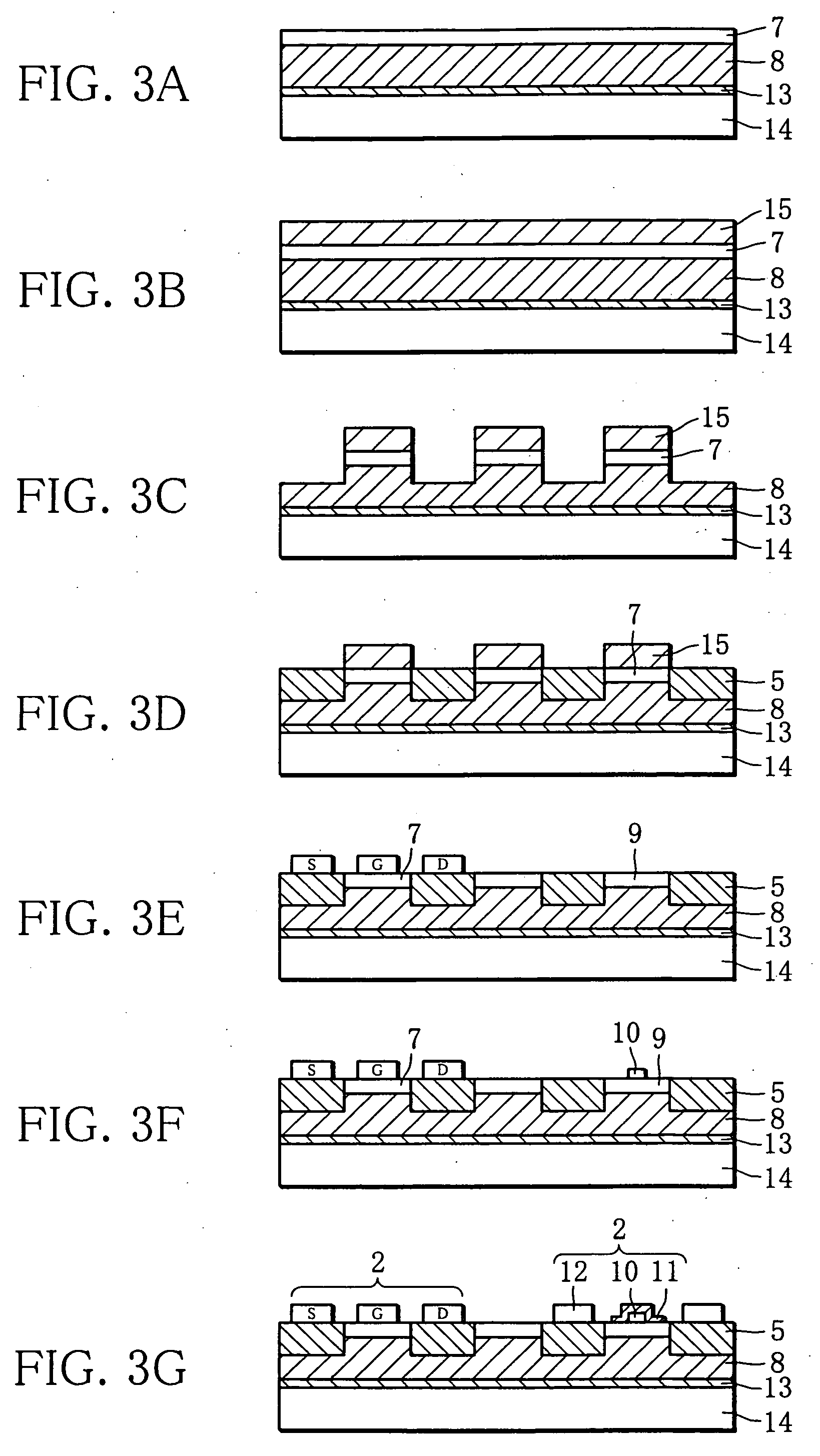
[0043] As described with reference to FIGS. 1 and 2, a GaN-based semiconductor integrated circuit 1 in embodiment 1 is so formed that two GaN-based semiconductor devices of different types, namely one FET 2 and one Schottky diode 3 form one unit (part surrounded by the dotted line in FIG. 2), and that four of such units are integrated. The size of the GaN-based semiconductor integrated circuit 1 having the plane structure shown in FIG. 1 is 10 mm×5 mm, which about one tenth of the size of the Si-based semiconductor integrated circuit having about the same power capacity.

[0044] The FET 2 has a channel layer 4 consisting of a semiconductor layer (electron supply layer) 7 of Al0.2Ga0.8N of thickness 30 nm and a semiconductor layer (electron transfer layer) 8 of GaN of thickness 400 nm. Contact layers 5, 5 of n-type GaN on either side of the channel layer 4 are embedded in etched grooves formed in the channel layer 4 by etching. The contact layers 5, 5 are the regions for taking out ca...

embodiment 2

[0060] The GaN-based semiconductor integrated circuit according to the present invention can be also as follows: As shown in FIG. 9, this GaN-based semiconductor integrated circuit 1 is formed by integrating, on an Si substrate 19, a GaN-based semiconductor circuit 1 in embodiment 1, an Si-based IGBT 16 as commonly used, and an Si-based FET 17. In the Figure, reference signs A, C, S, D and G represent an anode, a cathode, a source electrode, a drain electrode, and a gate electrode, respectively.

[0061] The GaN-based semiconductor integrated circuit in this embodiment is produced as follows:

[0062] [1] Using ultrahigh vacuum apparatus having a growth chamber and a patterning chamber, an epitaxial wafer is made by the molecular beam epitaxial method, as follows: First, on a semi-insulating Si substrate 19, an AlN layer 18 of thickness 50 nm is formed at growth temperature 640° C. using nitrogen in the form of free radical (7×10⁻³ Pa) and Al (1×10⁻⁵ Pa). Then, the Si substrate 19 is ca...


PUM


Abstract

A GaN-based semiconductor integrated circuit comprising a plurality of types of GaN-based semiconductor devices integrated on a single substrate, and one of the plurality of types of GaN-based semiconductor devices includes a Schottky diode. The Schottky diode includes a GaN-based semiconductor layer, a first anode and a second anode, wherein the first anode is joined to the GaN-based semiconductor layer to form a Schottky junction with a width smaller than the width of the GaN-based semiconductor layer, the second anode is joined to the GaN-based semiconductor layer to form a Schottky junction in a region other than the region in which the first anode is in contact with the GaN-based semiconductor layer, and electrically connected with the first anode, and the Schottky barrier formed between the second anode and the GaN-based semiconductor layer is higher than the Schottky barrier formed between the second anode and the GaN-based semiconductor layer.

Description

BACKGROUND OF THE INVENTION [0001] 1. Field of the Invention [0002] This invention relates to a semiconductor integrated circuit comprising a plurality of types of GaN-based semiconductor devices integrated on a substrate, and in particular, a GaN-based semiconductor integrated circuit suited to be used for large power conversion. [0003] 2. Description of the Related Art [0004] A power conversion device such as an inverter or a converter used in a power module for power conversion is formed using a semiconductor integrated circuit. Such power conversion device has a device structure shown in FIG. 10A, for example. As seen in FIG. 10B which shows the equivalent circuit thereof, the power conversion device is formed as an integrated circuit including a combination of an IGBT (insulated gate bipolar transistor) and a diode, each mainly made from Si-based semiconductors. The semiconductor integrated circuit including a combination of an IGBT and a diode is described in detail in “Design...

Claims


Application Information

Patent Timeline
IPC IPC(8): H01L29/76
CPCH01L21/8252H01L27/0605H01L27/0629H01L29/2003H01L29/417H01L29/475H01L29/7395H01L29/872
Inventor YOSHIDA, SEIKOH
Owner FURUKAWA ELECTRIC CO LTD
Why Eureka
Try Eureka