
Surface treated copper foil and circuit board

Inactive Publication Date: 2006-04-27
FURUKAWA ELECTRIC CO LTD
View PDF12 Cites 23 Cited by
  • Summary
  • Abstract
  • Description
  • Claims
  • Application Information

AI Technical Summary

Benefits of technology

[0022] It is desired to provide surface treated copper foil having high frequency characteristic, capable of forming fine pattern, and having sufficient peel strength and circuit board using the foil.
[0023] The present invention was made to provide surface treated copper foil having high frequency characteristic, capable of forming fine pattern, and having sufficient peel strength, and a circuit board with it. A surface treated copper foil and a circuit board using the surface treated copper foil have been successfully developed in the present invention which are capable of obtaining sufficient peel strength against epoxy resin substrate and polyimide film generally used as insulating substrates, liquid crystal polymer film with little dielectric characteristics change due to its extremely low hygroscopic property, high thermostability endurable to soldering together with very low peel strength, and polyetheretherketone based substrate and forming fine pattern without increasing roughness on the copper foil surface.

Problems solved by technology

In recent years, flexible boards have become further complicated and polyimide film has come to be used in many cases.
However, there are disadvantages with polyimide film such as large change of dielectric characteristics when water is absorbed, and wide decline of the high frequency characteristic under a water absorbing environment.
These procedures are complicated and disadvantageous.
However, film formed by the liquid crystal polymer or polyetheretherketone based resin exhibits poor adhesiveness with copper foil, and peel strength to copper foil is weaker comparing with that of polyimide.
It is certain that this method suits to the object of enhancing peel strength, however, for high frequency characteristic, it is not preferable to increase the surface roughness Rz by increased amount of roughening particles with regard to the skin effect.
On the other hand, depending on the kind of liquid crystal polymer films, some film is unable to give correlation to the peel strength even with larger surface roughness Rz of surface treated copper foil.
It is also not suitable to increase the surface roughness Rz by larger and / or more adhering amount of roughening particles to enhance higher peel strength in these fine pattern wiring applications as above.
Although, peel strength can be also enhanced by making surface of untreated copper foil rougher and decreasing adhering amount of roughening particles, it is not suitable because the high frequency characteristic is diminished and forming of fine pattern becomes difficult.
However, when liquid crystal polymer is formed into a film, strength in the thickness direction declines extremely because rodlike molecules orient in the surface direction Therefore, in such copper foil, the liquid crystal polymer film is easily broken at near the interface with copper foil and as a result, sufficient peel strength cannot be obtained.
However, even by these methods, sufficient peal strength has not been obtained for copper foil having small surface roughness.

Method used


Image

  • Surface treated copper foil and circuit board
  • Surface treated copper foil and circuit board
  • Surface treated copper foil and circuit board

Examples


examples

[0076] Examples 1 through 12 were prepared by plating (with roughening treatment) for at least one time on the original foils 1, 2 to 3 in the baths A, B and C in order of bath 1 to 2 with the bath composition, bath temperatures and currents stated above. The surface shapes shown in Table 1 were obtained.

[0077] Furthermore, the roughening treated surface was subjected to Ni plating (in amount of 0.3 mg / dm2) and zinc plating (in amount of 0.1 mg / dm2), and additional chromate treatment was performed thereon.

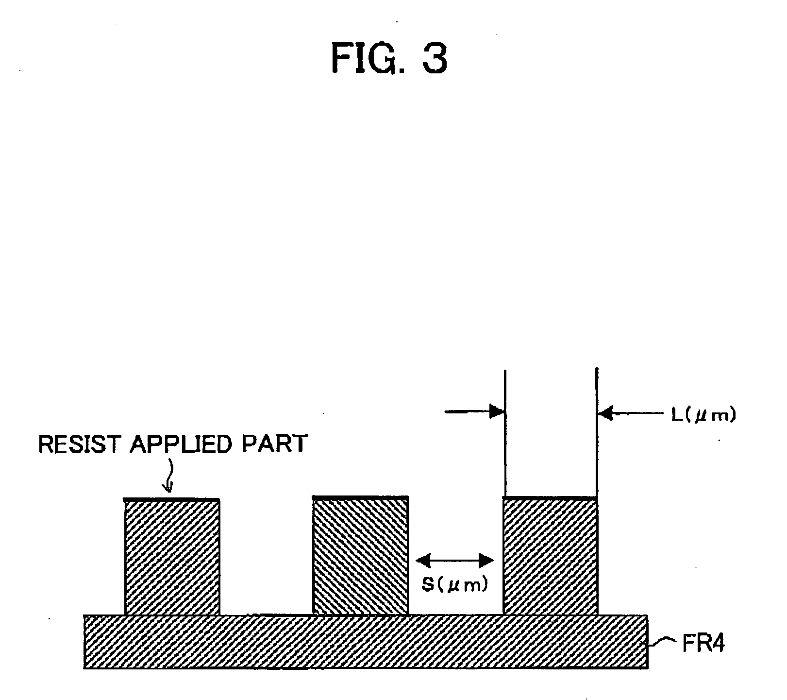
TABLE 1TreatedReductionFine patternExamplesElectro-surfacePeelrate ofcharacteristic:of PresentKind ofTreatedplatingOriginalroughnessNumber ofstrengthTransmissionminimum valuesInventioncopper foilsurfacebathfoil(μm)projectionBrightnessFilm(KN / m)loss (%)L / S (μm / μm)Example 1ElectrolyticMA11.127222Film 10.512514 / 14Example 2ElectrolyticSB31.855029Film 10.802820 / 20Example 3Rolling—B11.256422Film 10.571815 / 15Example 4ElectrolyticMB21.465824Film 10.533115 / 15Example 5ElectrolyticMA31.764...


PUM

PropertyMeasurementUnit
Lengthaaaaaaaaaa
Lengthaaaaaaaaaa
Surface roughnessaaaaaaaaaa

Abstract

A surface treated copper foil having high frequency characteristics, capable of forming fine pattern and having sufficient peel strength, wherein surface roughness Rz of roughening treated surface made by adhering roughening particles on at least one surface side of untreated copper foil is 0.6 to 1.5 μm and a brightness value is 35 or smaller; and a circuit board, on which wiring pattern is formed by the same surface treated copper foil, are provided.

Description

BACKGROUND OF THE INVENTION [0001] 1. Field of the Invention [0002] The present invention relates to a surface treated copper foil suitable to high frequency characteristic, formation of fine pattern and capable of keeping adhesiveness with insulating substrate while repressing the surface roughness, and furthermore relates to a circuit board using the surface treated copper foil. [0003] 2. Description of the Related Art [0004] As electronic equipments getting more compact and lighter, variety of recent electronic devices have become highly integrated. [0005] Composite materials for boards to produce flexible board, high-density mounting multilayer, board, and high-frequency circuit board (hereinafter, collectively referred to as circuit board or printed wiring board) are composed of a conductor (copper foil) and an insulating substrate (including film) to support it. The insulating substrate keeps insulation between the conductors and has strength to support the devices. [0006] Als...

Claims


Application Information

Patent Timeline
IPC IPC(8): B32B3/00H05K3/38
CPCC25D3/38C25D3/58C25D5/16C25D5/48C25D7/0614Y10T428/24917H05K2201/0355H05K2203/0307H05K2203/0723Y10T428/12472H05K3/384C25D5/627C25D5/605H05K3/38H05K3/22
Inventor SUZUKI, YUUJI
Owner FURUKAWA ELECTRIC CO LTD
Learn More