

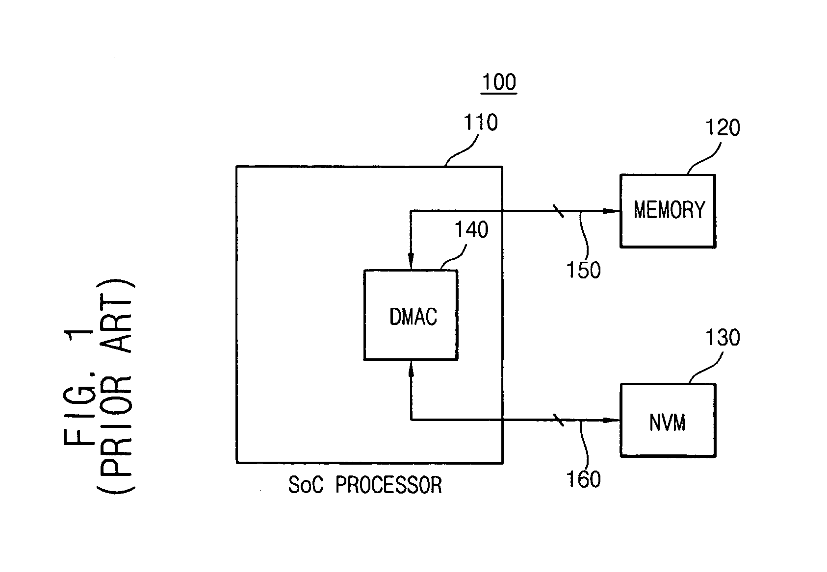
Microprocessor system with memory device including a DMAC, and a bus for DMA transfer of data between memory devices
a microprocessor and memory device technology, applied in digital storage, instruments, climate sustainability, etc., can solve the problems of inability to transfer data at a speed in excess of the processing speed of the cpu, processors are unavailable during such a large amount of data transfer, etc., to achieve the effect of increasing performance and reducing power consumption
- Summary
- Abstract
- Description
- Claims
- Application Information
AI Technical Summary
Benefits of technology
Problems solved by technology
Method used
Image

Examples
Embodiment Construction
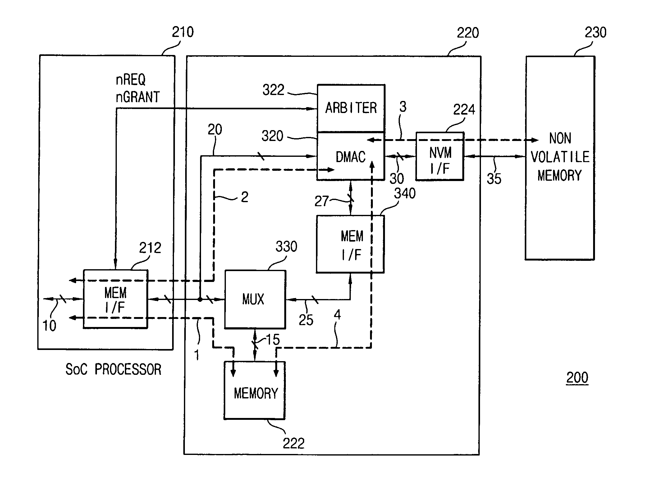
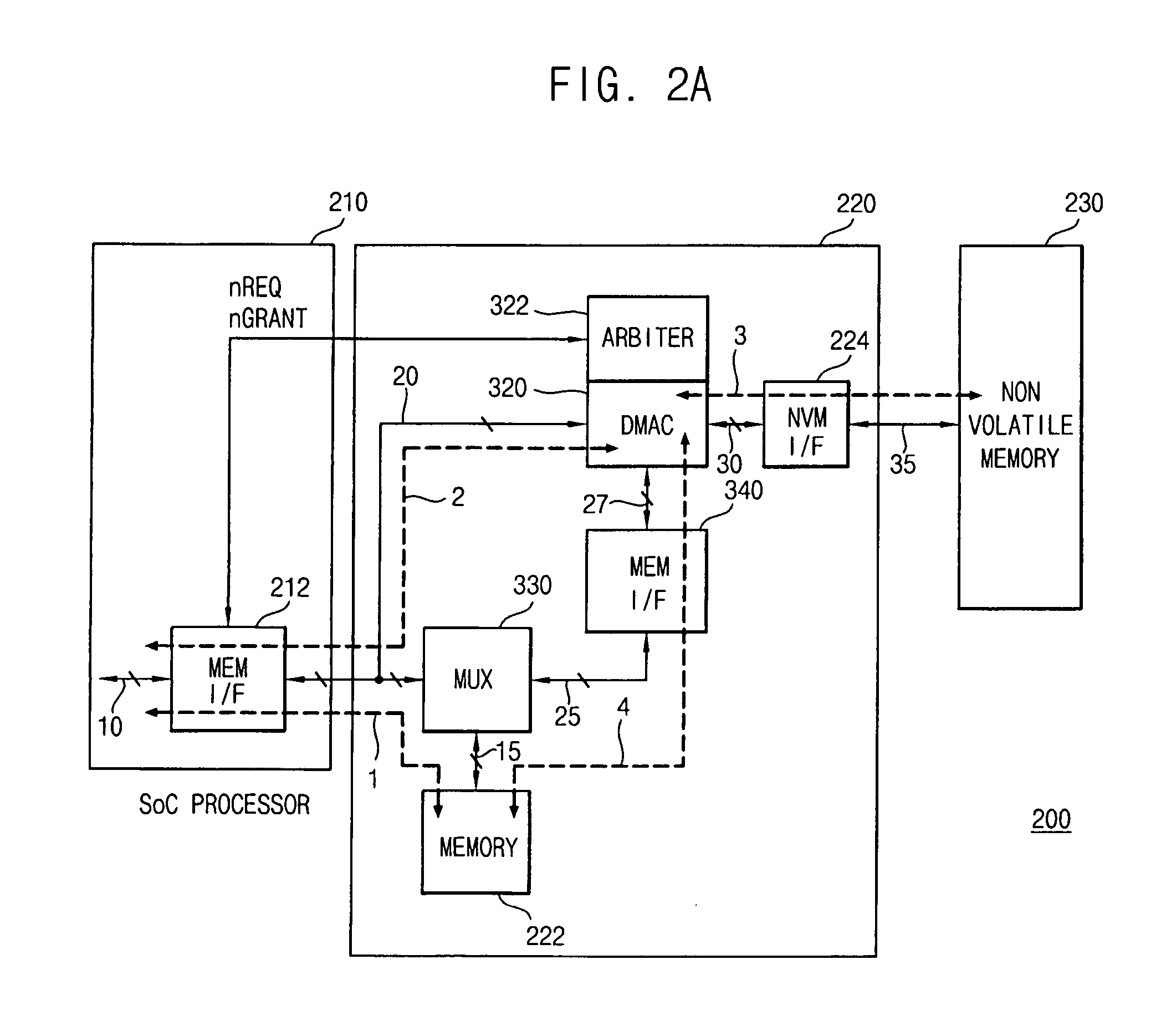
[0029]FIG. 2A is a circuit block diagram illustrating a processor system 200 including a memory device 220 having an internal (memory) bus 25, switchably connected (by a bus multiplexer 330) between a system memory (RAM) 222 and a direct memory access controller (DMAC 320), according to an embodiment of the present invention. The processor system 200 generally includes a “system-on-a-chip (SoC) processor 210, a memory device 220 (including a DMAC 320 with an Arbiter 322, and a bus multiplexer MUX 330), and an (external) nonvolatile memory (NVM) 230. The memory 222 may include synchronous DRAM cells or SRAM cells.
[0030]FIG. 2A additionally depicts, by dotted lines, the data routes (data transmission paths 1, 2, 3, &4) by which data may be transmitted to, from, and between the processor 210, the DMAC 320, the memory RAM 222 and the external nonvolatile memory NVM 230.
[0031] As depicted in FIG. 2A, data may be transmitted (e.g., written from the processor 210 into the system memory 2...
PUM
 Abstract
Description
Claims
Application Information