Light-emitting device having optical resonance layer
a light-emitting device and optical resonance technology, which is applied in the direction of solid-state devices, electric lighting sources, electric light sources, etc., can solve the problems of increased production costs, installation of mirrors, and the inability to easily form projection lenses on the substrate, so as to increase light coupling efficiency and brightness, and manufacture in a simple process , the effect of simple structur
- Summary
- Abstract
- Description
- Claims
- Application Information
AI Technical Summary
Benefits of technology
Problems solved by technology
Method used
Image

Examples
example 1
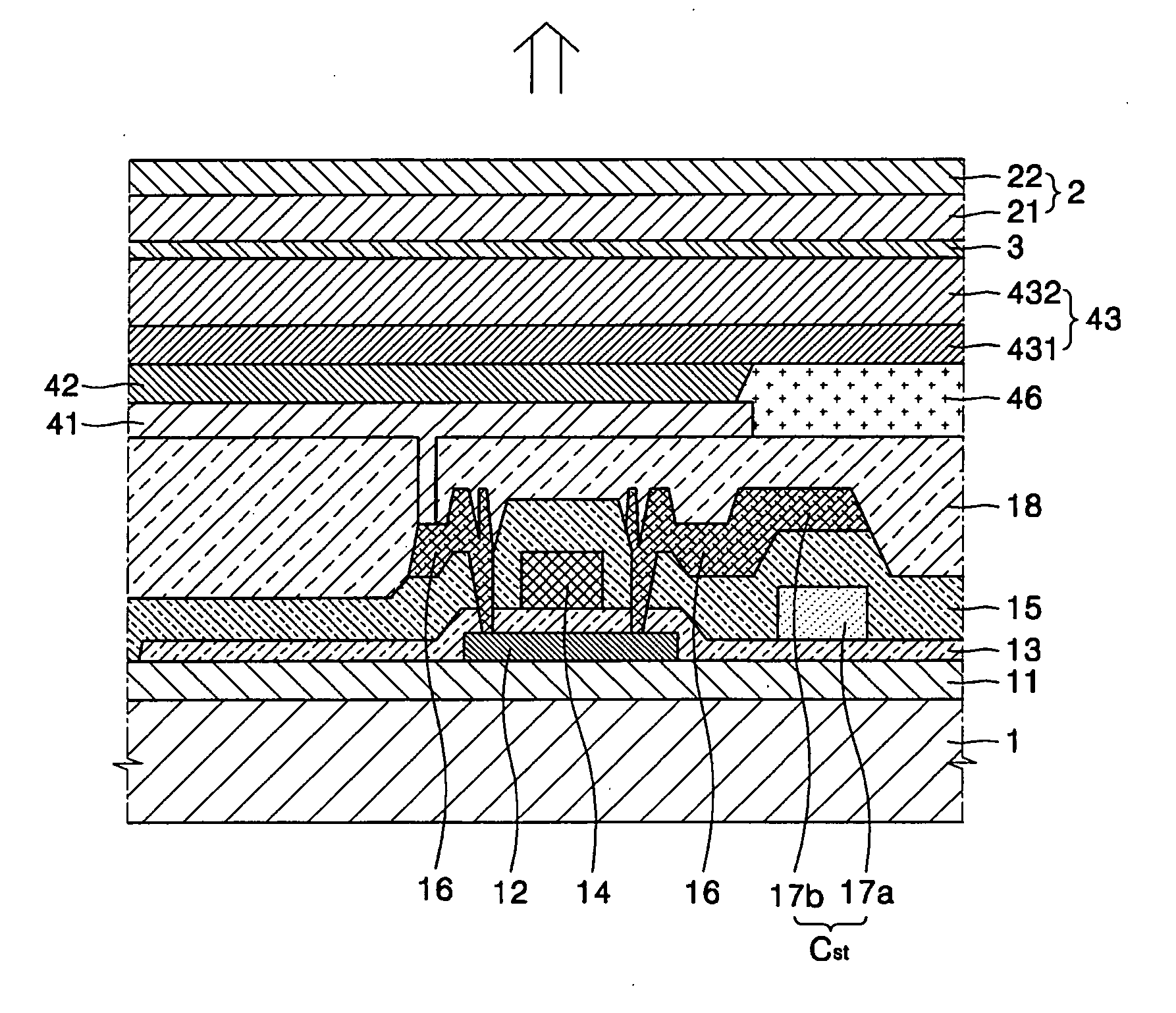
[0134] A test cell having 4 light-emitting regions each having a size of 2 mm×3 mm was prepared for estimation. First, a glass substrate was cleaned and NPS having a pore size of 10 nm or less was coated on the glass substrate.
[0135] Then, the coated substrate was heat-treated in an oven at 400° C. for 1 hour, thereby forming a first layer 21. The obtained first layer 21 had a refractive index of 1.2 and the thicknesses of the first layer 21 for the four regions was 0, 100, 230, and 300 nm. Then, an interlayer 3 made of SiO2 was deposited to a thickness of 20 nm using sputtering. The interlayer 3 had a refractive index of 1.45. When a porous material is used as a material of the first layer 21, the porous material typically absorbs moisture from the atmosphere, which deteriorates the lifetime of the organic light-emitting device. Thus, prior to depositing SiO2, the substrate was baked in a deposition chamber at 150° C. for 10 minutes to completely remove the absorbed moisture from ...
example 2
[0140] In this Example, a light-emitting device was manufactured in which the optical resonance layer 2 comprised the first layer 21 and the second layer 22 and its basic structure was the same as the embodiment illustrated in FIG. 1.
[0141] In this structure, a test cell was prepared in the same manner as in Example 1, except that a second layer 22 made of Si3N4 was formed on a substrate 1 using PECVD prior to forming the first layer 21. The formed second layer 22 had a refractive index of 2.0.
[0142]FIG. 13 shows a graph of a thickness of a second layer vs. rate of efficiency in the organic light-emitting obtained in Example 2. The three curves represent simulation results of the rate of efficiency when thicknesses of a first electrode layer 41, an interlayer 3, and the first layer 21 were set to 140 nm, 20 nm, and 340 nm, respectively, and a thickness of the second layer 22 was varied from 100 nm to 400 nm.
example 3
[0143] A light-emitting device with a similar structure as the device prepared in Example 2 was obtained. However, in Example 3, the thicknesses of a first electrode layer 41, an interlayer 3, and the first layer 21 were set to 160 nm, 20 nm, and 300 nm, respectively, and the thickness of the second layer 22 was varied from 100 nm to 400 nm. The three curves shown in FIG. 14 represent simulation results of the rate of efficiency versus the thickness of the second layer.
[0144] In Example 2, as illustrated in FIG. 13, the efficiency greatly increases in the Red (R) and Blue (B) pixels. In Example 3, as illustrated in FIG. 14, the efficiency increases in the R and B pixels at all thicknesses of the second layer 22, and efficiency increases for the G pixel at a majority of the simulated thicknesses
[0145] Color coordinates for the device obtained in Example 2 (FIG. 13) in which the second layer 22 has a thickness of 260 nm and for the device used as the Comparative Example (I) (FIG. 12...
PUM
 Abstract
Description
Claims
Application Information
 - R&D
- Intellectual Property
- Life Sciences
- Materials
- Tech Scout
- Unparalleled Data Quality
- Higher Quality Content
- 60% Fewer Hallucinations
Browse by: Latest US Patents, China's latest patents, Technical Efficacy Thesaurus, Application Domain, Technology Topic, Popular Technical Reports.
© 2025 PatSnap. All rights reserved.Legal|Privacy policy|Modern Slavery Act Transparency Statement|Sitemap|About US| Contact US: help@patsnap.com