

Semiconductor device and method of manufacturing the same
a technology of semiconductors and semiconductors, applied in the direction of semiconductor devices, basic electric elements, electrical equipment, etc., can solve the problems of difficult to reduce the active area of the active region, positional mismatch, and inability to reduce the manufacturing process steps, so as to reduce the steps of the photolithography process
- Summary
- Abstract
- Description
- Claims
- Application Information
AI Technical Summary
Benefits of technology
Problems solved by technology
Method used
Image

Examples
first embodiment
[0052] the present invention now will be explained.
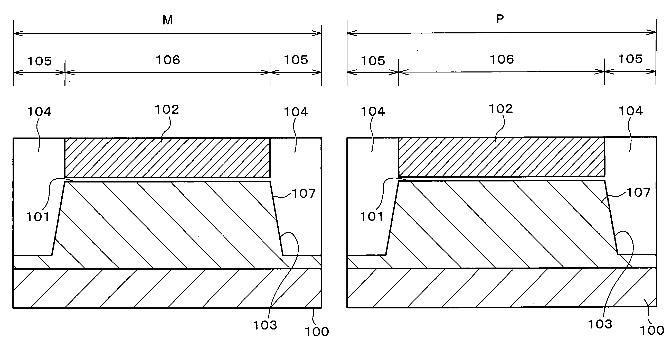
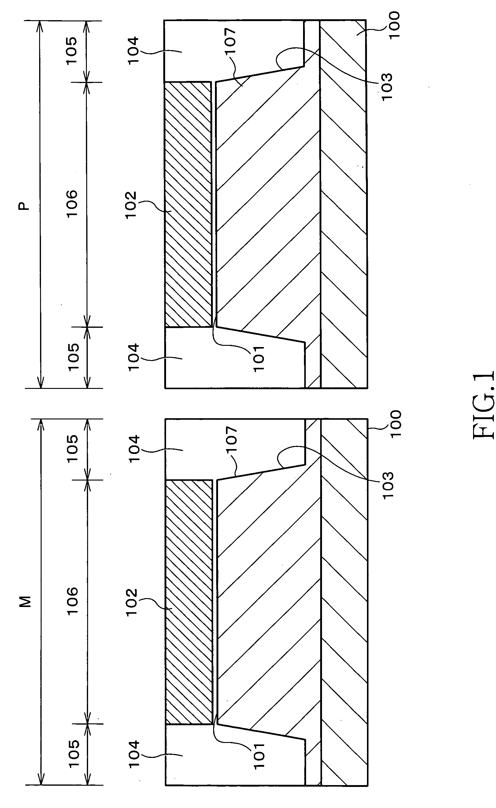
[0053] First, as shown in FIG. 1, a silicon oxide film 101 is formed on the surface of a semiconductor substrate 100 by thermal oxidation. Then, a silicon nitride film 102 is formed on the silicon oxide film 101 by chemical vapor deposition (CVD). The silicon nitride film 102 excluding a part of the film that becomes an active region is then removed. Accordingly, only the part of the surface of the semiconductor substrate 100 that becomes the active region is covered with the silicon nitride film 102. The silicon nitride film 102 patterned in this way is used as a “field-forming insulation film” that forms an isolation region.
[0054] Next, the silicon oxide film 101 and the semiconductor substrate 100 are etched using the silicon nitride film 102 that works as the field-forming insulation film as a mask, thereby forming an element isolation trench 103 having a depth of about 350 nm. The semiconductor substrate 100 is then thermally ...
second embodiment
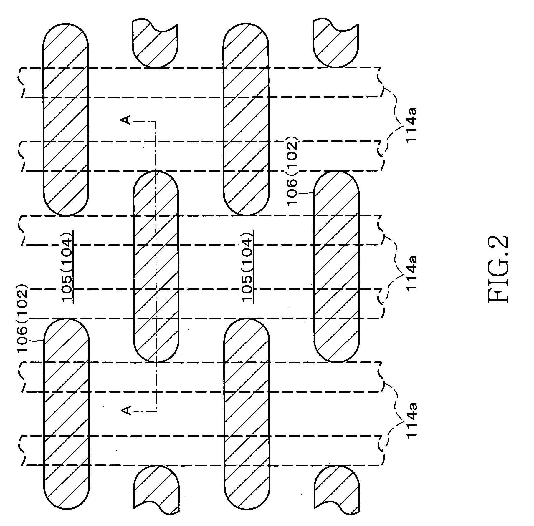
[0086] As explained above, it is necessary to etch the semiconductor substrate 100 (the p-type well layer 107) using the silicon nitride film 102 as a mask. Because a film thickness of the silicon nitride film 102 slightly reduces by this etching, the silicon nitride film 102 needs to be set with a slightly large thickness in advance. A large part of the sidewall formed at the stage of the boundary between the isolation region 105 and the active region 106 is removed at the time of forming the gate trench 214c. The sidewall can be removed to a level at which the gate wiring is not disconnected, in the cleaning process after the etching.
[0087] Next, as shown in FIG. 25, a gate insulation film 110 is formed on the surface of the gate trench 214c by thermal oxidation. After this, the polycrystalline silicon film 111, the tungsten nitride film 112, and the tungsten film 113 are deposited sequentially. In this case, the polycrystalline silicon film 111 and the tungsten nitride film 112 ...
third embodiment
[0095] Next, the mask pattern is removed, and a silicon oxide film 308 is formed in the film thickness of about 10 to 20 nm on the whole surface by LPCVD. The silicon oxide film 308 is then etched back as shown in FIG. 28, thereby forming a sidewall 308a. In this case, by sufficiently performing the over-etching, the gate trench 314a formed on the silicon oxide film 104 in the isolation region 105 can be further etched, thereby forming a deeper gate trench 314b. By performing this over-etching, the film thickness of the silicon nitride film 102 can be reduced substantially. Therefore, in the third embodiment, the film thickness of the silicon nitride film 102 needs to be set sufficiently large in advance.
[0096] Furthermore, as shown in FIG. 29, the semiconductor substrate 100 (the p-type well layer 107) is etched by using the silicon nitride film 102 and the sidewall 308a as masks, thereby further etching the gate trench 314a formed on the semiconductor substrate 100 (the p-well lay...
PUM
 Abstract
Description
Claims
Application Information