Vertical aligned nano-scale diamond structure and process for fabricating the same
- Summary
- Abstract
- Description
- Claims
- Application Information
AI Technical Summary
Benefits of technology
Problems solved by technology
Method used
Image
Examples
example a
Diamond Nanotips
Experimental Procedure
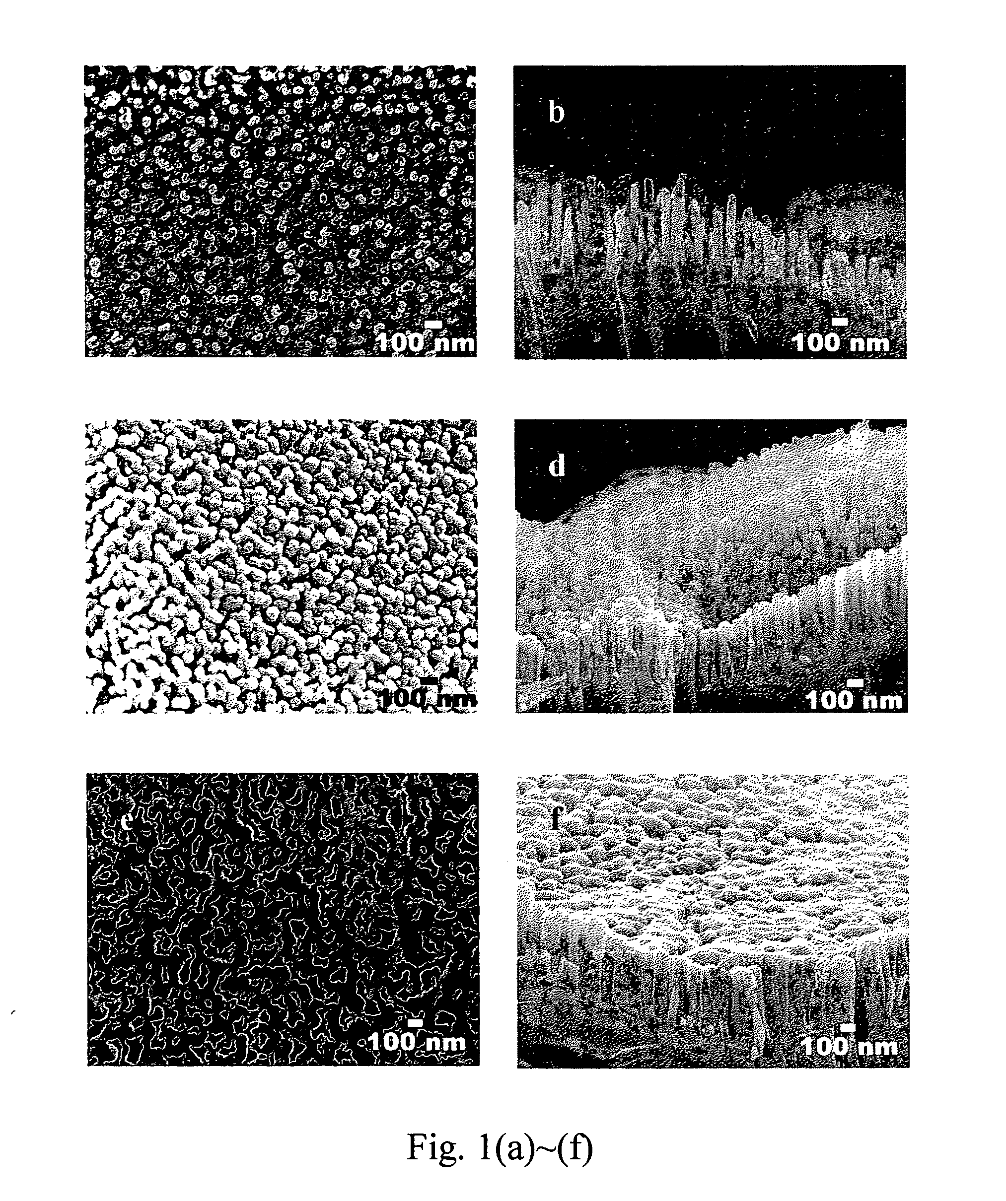
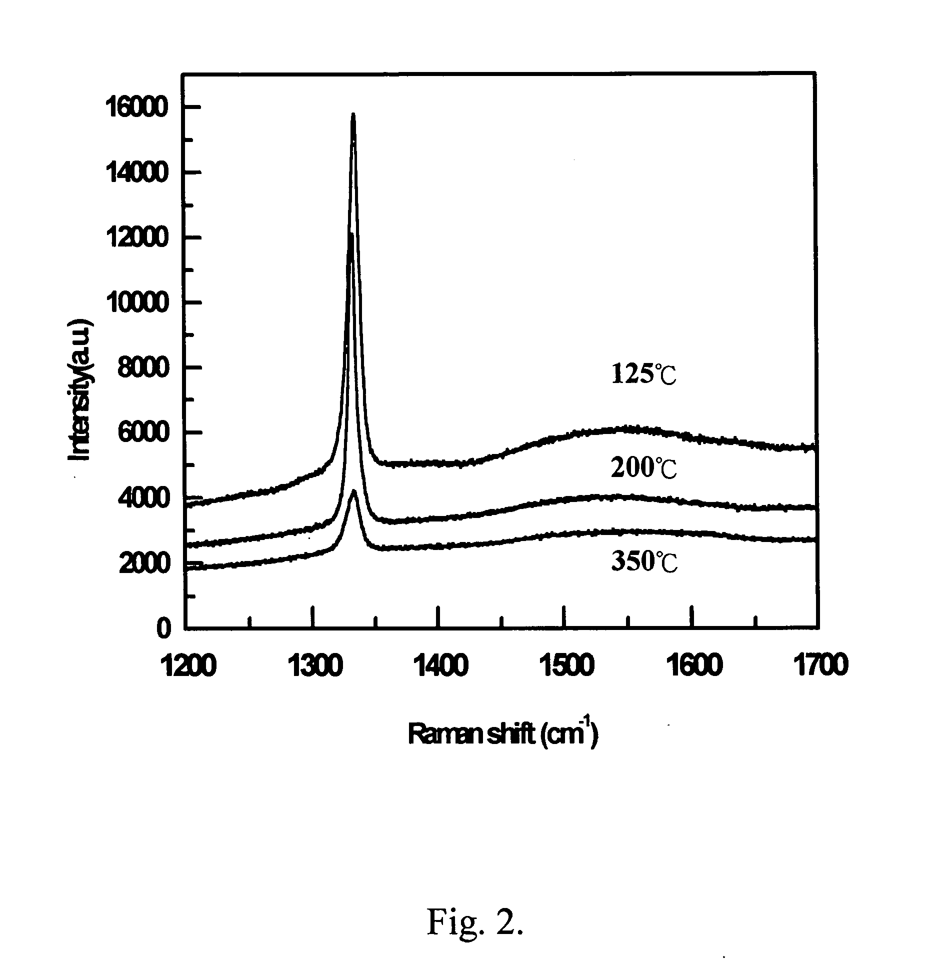
[0029] Diamond nanotips were grown on polycrystalline diamond / silicon (D / Si) substrates in a 2.54 GHz planar microwave plasma enhanced chemical vapor deposition (MPECVD) system. The polycrystalline D / Si substrate is about 540 μm thick and 5×5 mm2 in size. A planar-MPECVD chamber was pumped down to a base pressure of 4×10⁻² Torr, and a mixture of 30% CH4 and 70% H2 was fed into the chamber to ignite the CH4 / H2 mixed plasma at 3000 W and at a total pressure of 0.17 Torr. Nano-scale diamond tips were grown on the polycrystlline D / Si substrates at different substrate temperature (125° C.; 200° C. and 350° C.) and different bias voltages (−50V, −150V, and −250 V) for 2 hours. No metal catalysts are required for the growth at such low temperature. A field emission scanning electron microscope (FESEM) image was obtained by flashing ultra-thin Au onto nano-scale diamond tips because the tips are not conductors. Raman spectroscopy was used for the che...
example b
Diamond Nanotubes
Experimental Procedure
[0033] NDTs were synthesized on polycrystalline diamond substrate at bias voltage of −50 to −250 V in a 2.54 GHz planar microwave plasma enhanced chemical vapor deposition (MPECVD) system. The polycrystalline diamond substrate is approximate 90 μm thick and 5×5 mm2 in size. In a typical experiment, MPECVD chamber was pumped down to a base pressure of 3.5×10⁻³ torr, and a mixture of 30% CH4 and 70% H2 was fed into the chamber to ignite the CH4 / H2 mixed plasma at 3,000 W and at a total pressure of 0.13 torr. The process time ranges from 0.5 to 2 hour. The substrate temperature Ts was heated by plasma bombardment during growth and determined to be ˜200° C. at the end of each run. No metal catalysts are required to grow NDTs at such low temperature. A transmission electron microwaves (TEM, JEM-4000EX, operated at 400 kV) was used to characterize the morphologies and crystal structures of NDTs. A better field emission scanning electron microscope...
example c
[0037] The heat spreading performance of NDTs according to this invention is shown in FIG. 7, and IR apparatus to detect that is arranged as FIG. 6. As shown in FIG. 6, a heat spreader made of NDTs lay upon the plate of IR detector, which a specific temperature of plate is set, and the surface temperature of heat spreader, Ts, is detected by IR, therefore the temperature difference between the plate and Ts is calculated and the heat spreading performance for the heat spreader also can be achieved. In order to change the conditions and to observe the results when the forced convention of heat is applied by using an air fan, the heat spreading performance for the heat spreader due to several times of area for heat transfer, namely fins of NDTs, becomes more obvious than that of a diamond film.
[0038] As shown in FIG. 7, the heat spreading performance of NDTs / diamond according to this invention is superior to that of a single diamond film in several times of effective con...
PUM
 Abstract
Description
Claims
Application Information


