Method and apparatus for preventing metal/silicon spiking in MEMS devices

a technology of metal/silicon spiking and mems devices, which is applied in the manufacture of microstructural devices, electrical apparatus, and semiconductor devices, etc., can solve problems such as adverse effects on the underlying devices, and achieve the effect of preventing spiking

Inactive Publication Date: 2006-05-25
TAIWAN SEMICON MFG CO LTD
View PDF14 Cites 16 Cited by
  • Summary
  • Abstract
  • Description
  • Claims
  • Application Information

AI Technical Summary

Benefits of technology

[0005] In another embodiment, the disclosure relates to a method for preventing extrusion of metal along the contact walls of a MEMS device formed on a silicon wafer. The method includes providing a substrate having the MEMS structure thereon, the MEMS structure defined by a metallization layer interposed between a first barrier layer and a second barrier layer, the first barrier layer interfacing the substrate and a bottom surface of the metallization layer and the second barrier layer interfacing a top surface of the metallization layer, the MEMS structure having a top surface and at least two sidewalls; forming one or more spacer layers to conceal each of the sidewalls; and depositing a silicon layer to substantially cover the spacer structure, the metallization layer being separated from the silicon layer at each side by at least one of the spacers or the barrier layers.
[0006] In still another embodiment, the disclosure relates to a Micro-Electro-Mechanical device having electrical components formed on an integrated circuit wafer. A method for eliminating extrusion of metallic atoms of the MEMS device onto a silicon layer of the IC wafer includes providing a substrate having the MEMS structure thereon, the MEMS structure defined by a metallization layer interposed between a first barrier layer and a second barrier layer, the first barrier layer interfacing the substrate and a bottom surface of the metallization layer and the second barrier layer interfacing a top surface of the metallization layer, the MEMS structure having a top surface and at least two sidewalls; using oxygen plasma to form a plurality of spacers to cover the at least two side walls of the MEMS structure; growing amorphous silicon over the substrate to substantially cover the spacer structure, the metallization layer being separated from the amorphous silicon layer by at least one of the spacers or the barrier layers.
[0007] In yet another embodiment, the disclosure relates to preventing spiking between metallic portions of a MEMS device and an IC wafer by providing a substrate having the MEMS structure thereon, the MEMS structure defined by a metallization layer interposed between a first barrier layer and a second barrier layer, the first barrier layer interfacing the substrate and a bottom surface of the metallization layer and the second barrier layer interfacing a top surface of the metallization layer, the MEMS structure having a top surface and at least two sidewalls; using thermal oxidation to form a plurality of spacers to cover the at least two side walls of the MEMS structure; growing amorphous silicon over the substrate to substantially cover the spacer structure, the metallization layer being separated from the amorphous silicon layer by at least one of the spacers or the barrier layers.

Problems solved by technology

Extrusion is a defect and can have adverse affects on the underlying device.

Method used


Image

  • Method and apparatus for preventing metal/silicon spiking in MEMS devices
  • Method and apparatus for preventing metal/silicon spiking in MEMS devices
  • Method and apparatus for preventing metal/silicon spiking in MEMS devices

Examples


Embodiment Construction

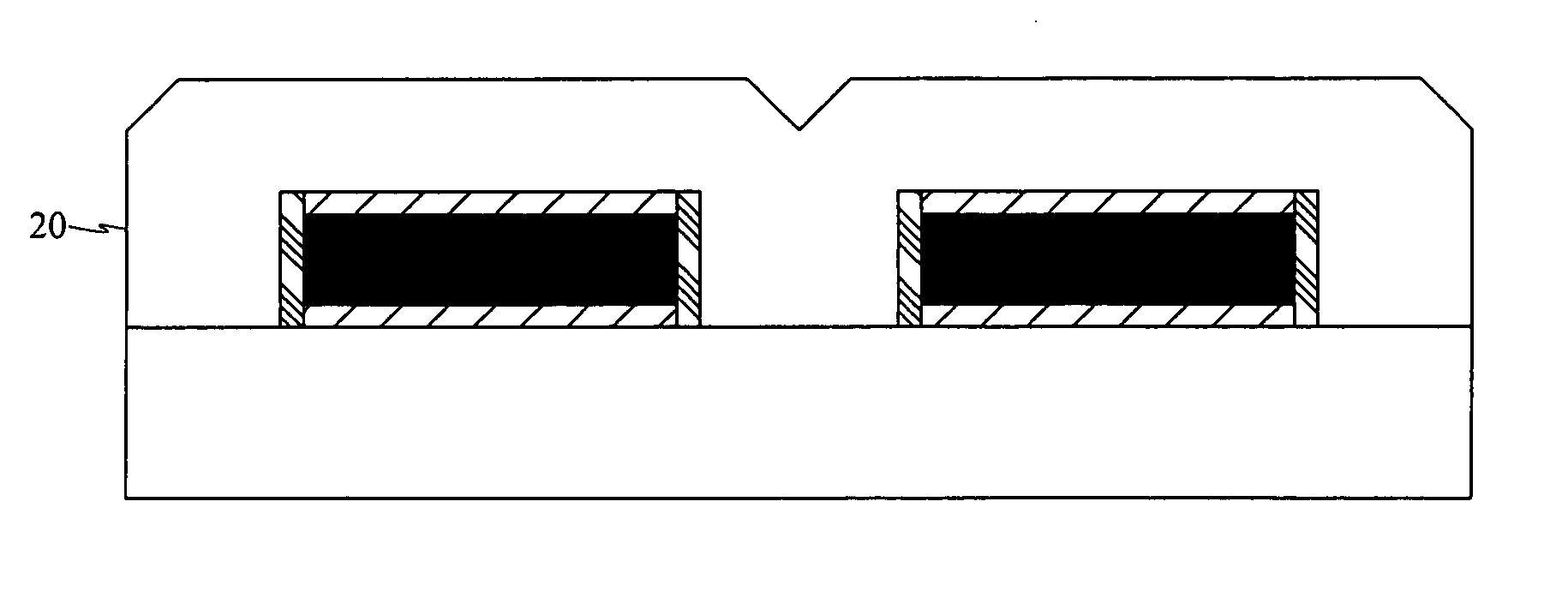
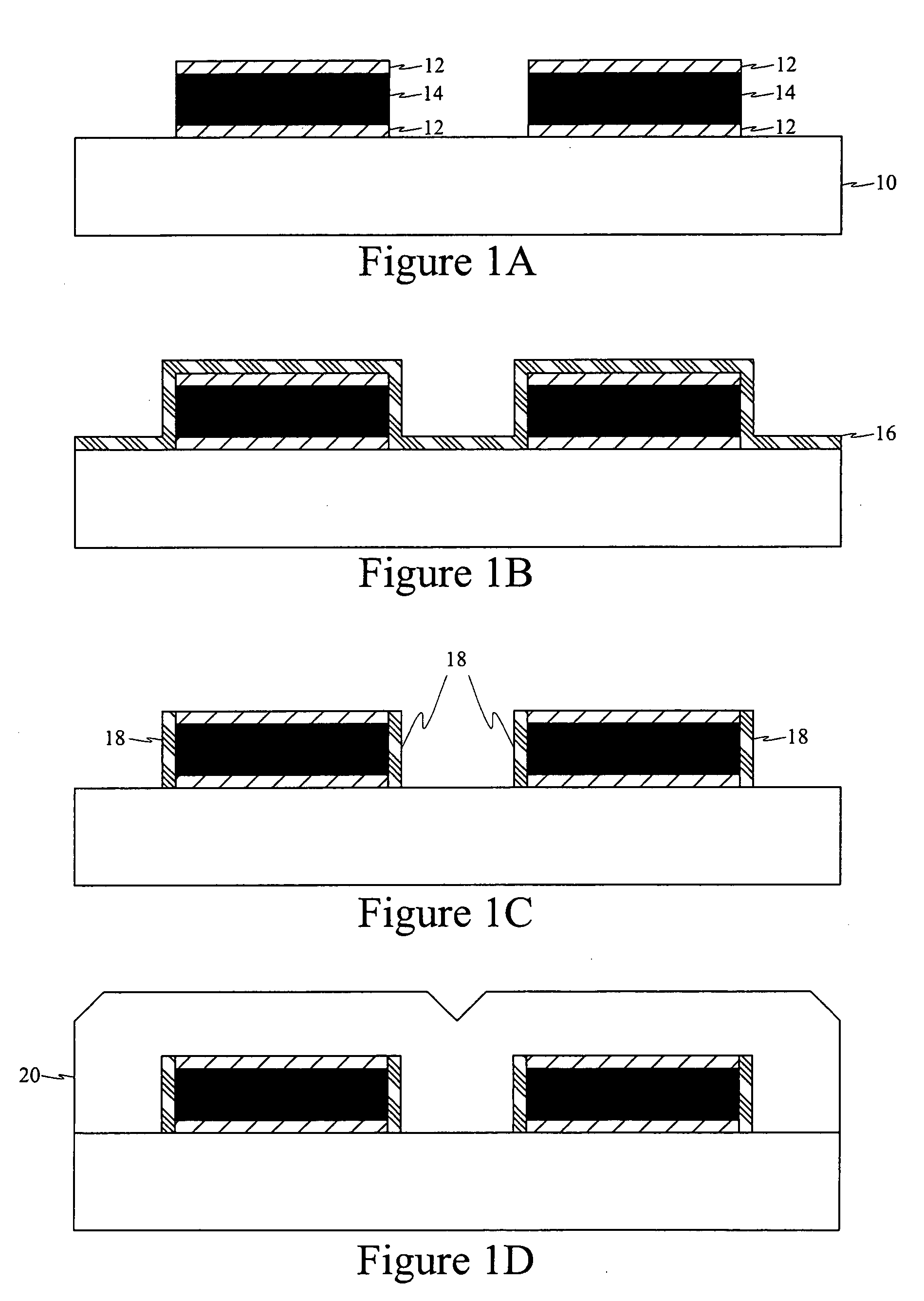
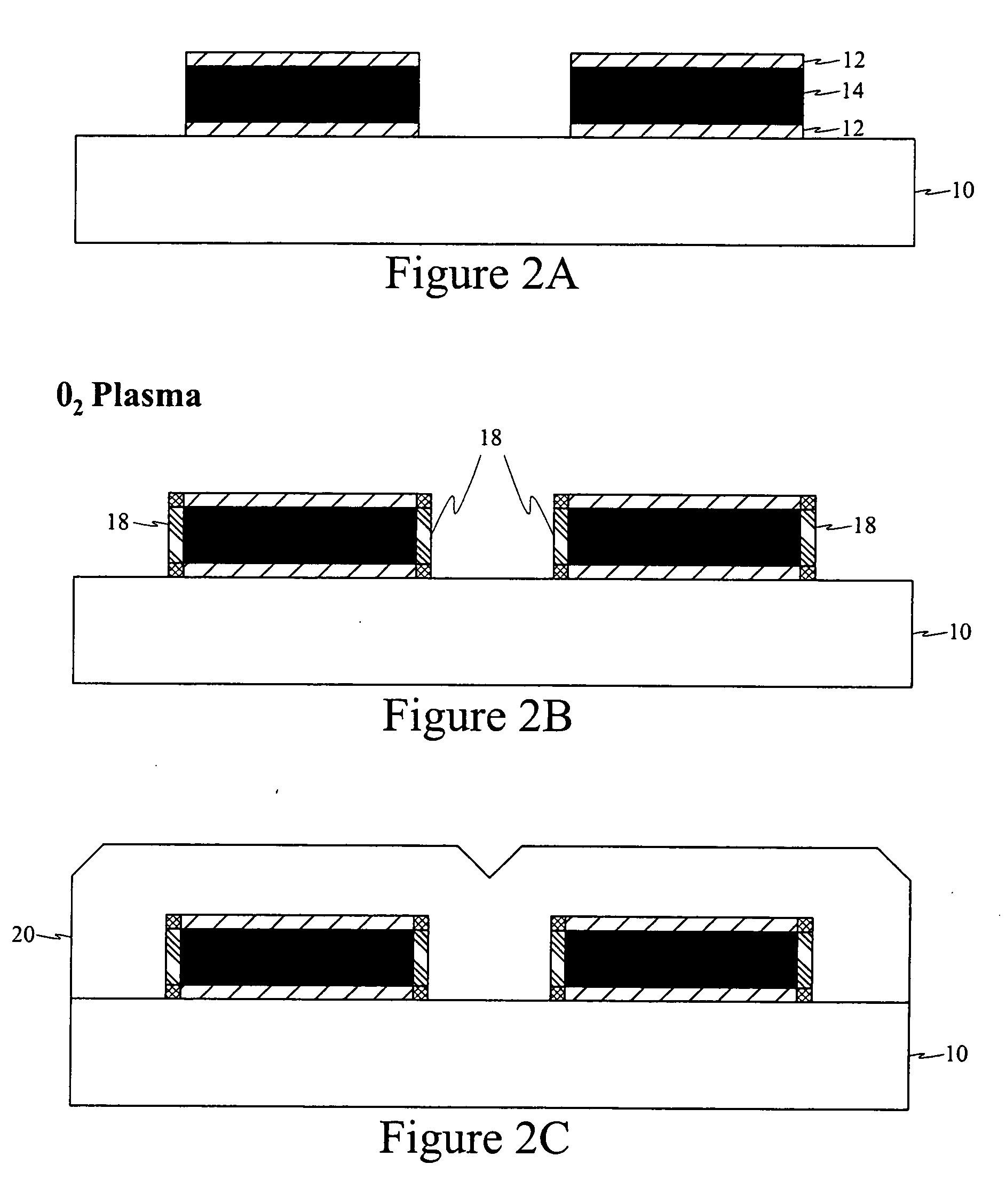
[0011]FIG. 1 schematically illustrates a method for preventing extrusion according to one embodiment of the disclosure. Referring to FIG. 1A, substrate 10 is provided having deposited thereon barrier layers 12 and the conductive layers 14. Substrate 10 can include conventional semiconductor material such as silicon. Semiconductor substrate 10 may have a plurality of MOS transistors (not shown) incorporated therein. The barrier layer can be formed from titanium nitride (TiN), titanium (Ti), tungsten nitride (WN), an alloy of titanium and tungsten (Ti / W), silicon dioxide or silicon nitride. The barrier layer serves to prevent spiking (or extrusion) between the conductive layers (interchangeably, the metallization layers) 14 and substrate 10. In one embodiment, the barrier layer has a thickness of about 200-500 Angstroms. The barrier layers can be deposited using conventional deposition techniques including CVD or PVD.

[0012] The metallization layer 14 can be formed from aluminum, copp...


PUM

PropertyMeasurementUnit
temperatureaaaaaaaaaa
thicknessaaaaaaaaaa
dielectricaaaaaaaaaa

Abstract

The disclosure relates to a method and apparatus for preventing extrusion or spiking of a metal atom from a metallization layer to other layers of a silicon wafer. In one embodiment, the method includes forming a silicon-on-ship device with a MEMS component on the substrate. The MEMS component may include one or more metal or metallic alloys. To prevent spiking from the MEMS component, the sides thereof can be coated with one ore more spacer or barrier layers. In one embodiment, oxygen plasma and thermal oxidation methods are used to deposit spacers. In another embodiment, an oxide layer is deposited over the wafer, covering the substrate and the MEMS component. Selective etching or anisotropic etching can be used to remove the oxide layer from certain regions of the MEMS and the substrate while covering the sidewalls. An amorphous silicon layer can then be deposited to cover the MEMS device.

Description

BACKGROUND [0001] A Micro-Electro-Mechanical (“MEMS”) device defines the integration of electromechanical elements on a common silicon substrate through micro-fabrication technology. The electrical elements such as complementary metal oxide semiconductor (“CMOS”) or bipolar devices are fabricated on an underlying silicon substrate using integrated circuit (“IC”) processes while the micro-mechanical components are fabricated by micro-machining processes that selectively etch away regions of the silicon substrate. The machining of the mechanical devices on the same silicon substrate results in a complete system-on-a-chip technology. [0002] The process steps and sequences needed for MEMS can present possible vulnerabilities for the semiconductor device components of MEMS. Such problems do not arise in traditional semiconductor fabrications. For example, amorphous silicon is used for the sacrificial layer in MEMS devices. The sacrificial amorphous silicon material may directly interface...

Claims


Application Information

Patent Timeline
Patent Type & Authority Applications(United States)
IPC IPC(8): H01L21/00H01L31/0203
CPCB81C1/00253B81C2201/0178B81C2201/053
Inventor CHANG, YUH-HWACHEN, FEI-YUNTZENG, JIANN-TYNGCHU, CHENG-YUPENG, CHUN-KAIYEH, CHIH-CHIEHPO, CHIH-HENGHO, DAH-CHUEN
Owner TAIWAN SEMICON MFG CO LTD
Why Eureka
Try Eureka