Thermal interface material and method for manufacturing same

a technology applied in the field of thermal interface materials and manufacturing methods, can solve the problems of inadequately meeting the heat dissipation requirements of modern electronic components, the heat conduction coefficient of thermal interface materials is now considered too low for many contemporary applications, and the value of heat conduction coefficient cannot be increased, so as to achieve excellent heat conduction, reduce thickness, and good flexibility

Inactive Publication Date: 2006-06-08
HON HAI PRECISION IND CO LTD
View PDF3 Cites 62 Cited by
  • Summary
  • Abstract
  • Description
  • Claims
  • Application Information

AI Technical Summary

Benefits of technology

[0011] Accordingly, an object of the present invention is to provide a thermal interface material having a reduced thickness, good flexibility and excellent heat conduction.
[0019] Unlike in a conventional thermal interface material, the carbon nanotubes of the thermal interface material of the present invention are disposed in the silver colloid base uniformly and directionally. Thus, each carbon nanotube of the thermal interface material can provide a heat conduction path in a direction perpendicular to a main heat absorbing surface of the thermal interface material. This ensures that the thermal interface material has a high heat conduction coefficient. Furthermore, the carbon nanotubes have nanometer-scale silver filled therein, and this further enhances the thermal conductivity and heat conduction stability.

Problems solved by technology

However, a heat conduction coefficient of the thermal interface material is now considered to be too low for many contemporary applications, because it cannot adequately meet the heat dissipation requirements of modern electronic components.
The value of the heat conduction coefficient cannot be increased, because the thickness cannot be reduced.
However, the thermal interface material formed by injection molding is relatively thick.
This increases a bulk of the thermal interface material and reduces its flexibility.
This means that heat does not necessarily spread uniformly through the thermal interface material.

Method used


Image

  • Thermal interface material and method for manufacturing same
  • Thermal interface material and method for manufacturing same

Examples


Embodiment Construction

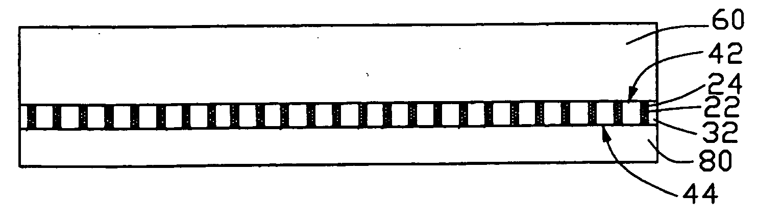
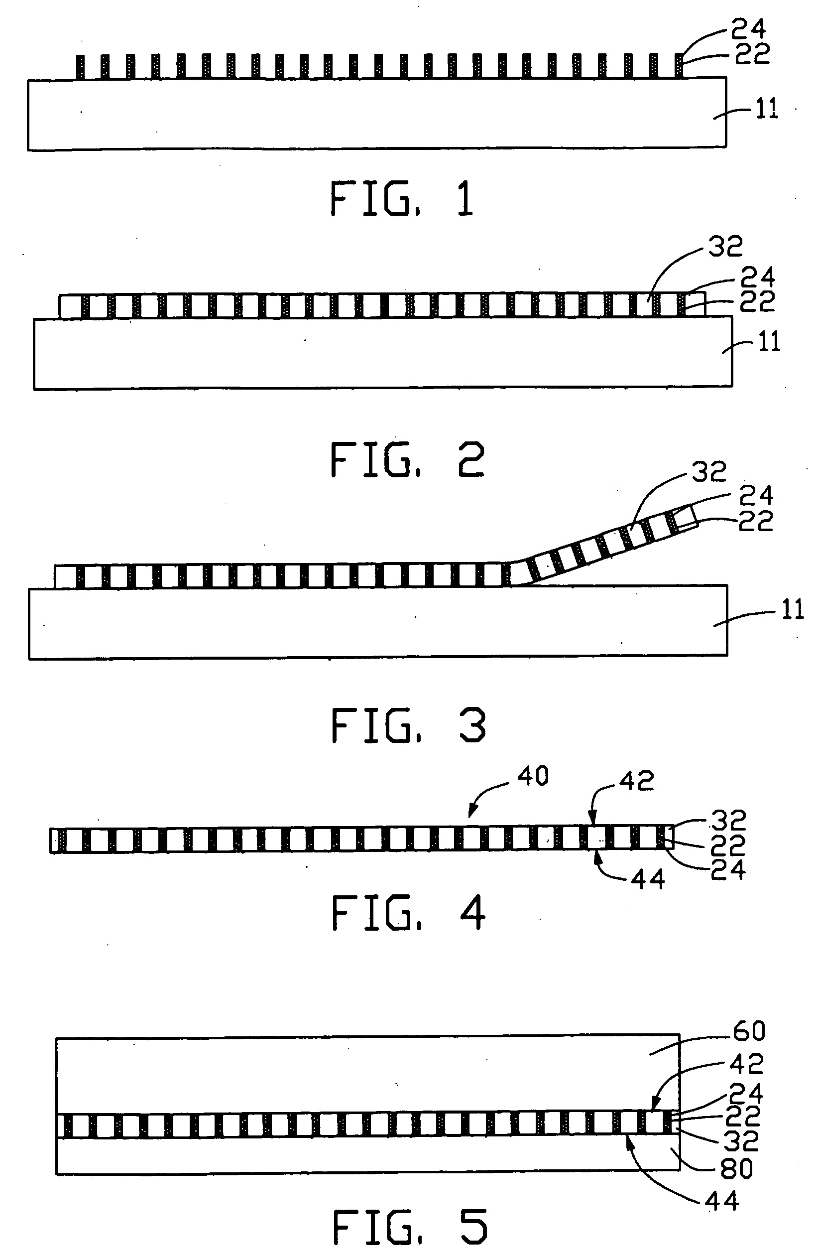
[0026] Referring to FIG. 1, an array of carbon nanotubes 22 having nanometer-scale silver 24 filled therein is shown. The carbon nanotubes 22 are substantially parallel to each other and directionally formed on a substrate 11.

[0027] In a preferred method of the present invention, the carbon nanotubes22 with the nanometer-scale silver 24 filled therein are manufactured as follows. Firstly, the substrate 11 is provided. The substrate 11 can be made of glass, quartz, silicon, or alumina. In the preferred method, the substrate 11 is made of porous silicon. A surface of the porous silicon is a porous layer. Diameters of apertures in the porous layer are extremely small, generally about 3 nanometers. Then a catalyst film (not shown) is uniformly deposited on the substrate 11 by thermal disposition, electron-beam disposition, or sputtering. The catalyst film 12 can be made of iron (Fe), cobalt (Co), nickel (Ni), or an alloy thereof. In the preferred method, the catalyst film 12 is made of...


PUM

PropertyMeasurementUnit
thicknessaaaaaaaaaa
diametersaaaaaaaaaa
thicknessaaaaaaaaaa

Abstract

A thermal interface material (40) includes a silver colloid base (32), and an array of carbon nanotubes (22) disposed in the silver colloid base uniformly. The carbon nanotubes have nanometer-scale silver filled therein, are substantially parallel to each other, and extend from a first surface (42) to a second surface (44) of the thermal interface material. A method for manufacturing the thermal interface material includes the steps of: (a) forming an array of carbon nanotubes with nanometer-scale silver filled therein on a substrate; (b) submerging the carbon nanotubes in a silver colloid base; (c) solidifying the silver colloid base; and (d) peeling the solidified silver colloid base with the carbon nanotubes secured therein off from the substrate.

Description

BACKGROUND OF THE INVENTION [0001] 1. Field of the Invention [0002] The invention relates generally to thermal interface materials and manufacturing methods thereof; and more particularly to a kind of thermal interface material which conducts heat by using carbon nanotubes, and a manufacturing method thereof. [0003] 2. Description of Related Art [0004] Electronic components such as semiconductor chips are becoming progressively smaller, while at the same time heat dissipation requirements thereof are increasing. Commonly, a thermal interface material is utilized between the electronic component and a heat sink in order to efficiently dissipate heat generated by the electronic component. [0005] A conventional thermal interface material is made by diff-using particles with a high heat conduction coefficient in a base material. The particles can be made of graphite, boron nitride, silicon oxide, alumina, silver, or other metals. However, a heat conduction coefficient of the thermal int...

Claims


Application Information

Patent Timeline
Patent Type & Authority Applications(United States)
IPC IPC(8): H01L29/06H01L23/14
CPCB82Y10/00H01L23/373H01L2924/0002Y10T428/26Y10T428/30H01L2924/00
Inventor LEU, CHARLESYU, TAI-CHENGCHEN, GA-LANE
Owner HON HAI PRECISION IND CO LTD
Why Eureka
Try Eureka