

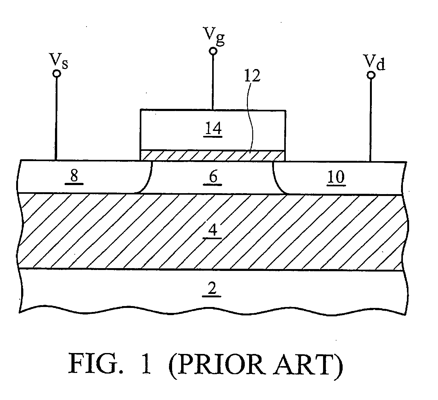
Capacitor-less 1T-DRAM cell with Schottky source and drain
a technology of capacitors and source, applied in the direction of transistors, electrical apparatus, semiconductor devices, etc., can solve the problems of degrading device reliability, no hot carrier generated, etc., and achieve the effect of enhancing device reliability and better scaling capability for suppressing short channel effects
- Summary
- Abstract
- Description
- Claims
- Application Information
AI Technical Summary
Benefits of technology
Problems solved by technology
Method used
Image

Examples
Embodiment Construction
[0020] The making and using of the presently preferred embodiments are discussed in detail below. It should be appreciated, however, that the present invention provides many applicable inventive concepts that can be embodied in a wide variety of specific contexts. The specific embodiments discussed are merely illustrative of specific ways to make and use the invention, and do not limit the scope of the invention.
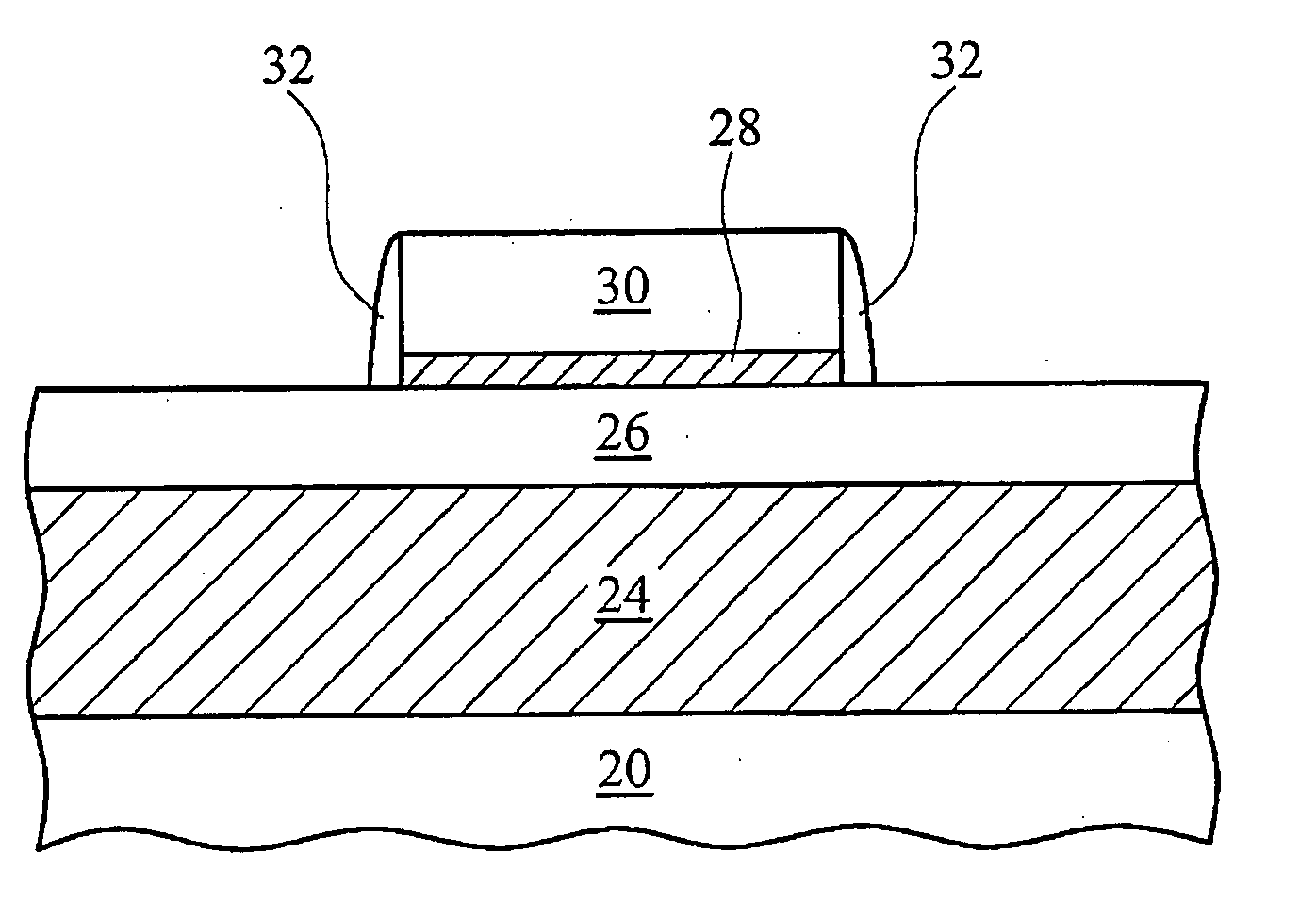
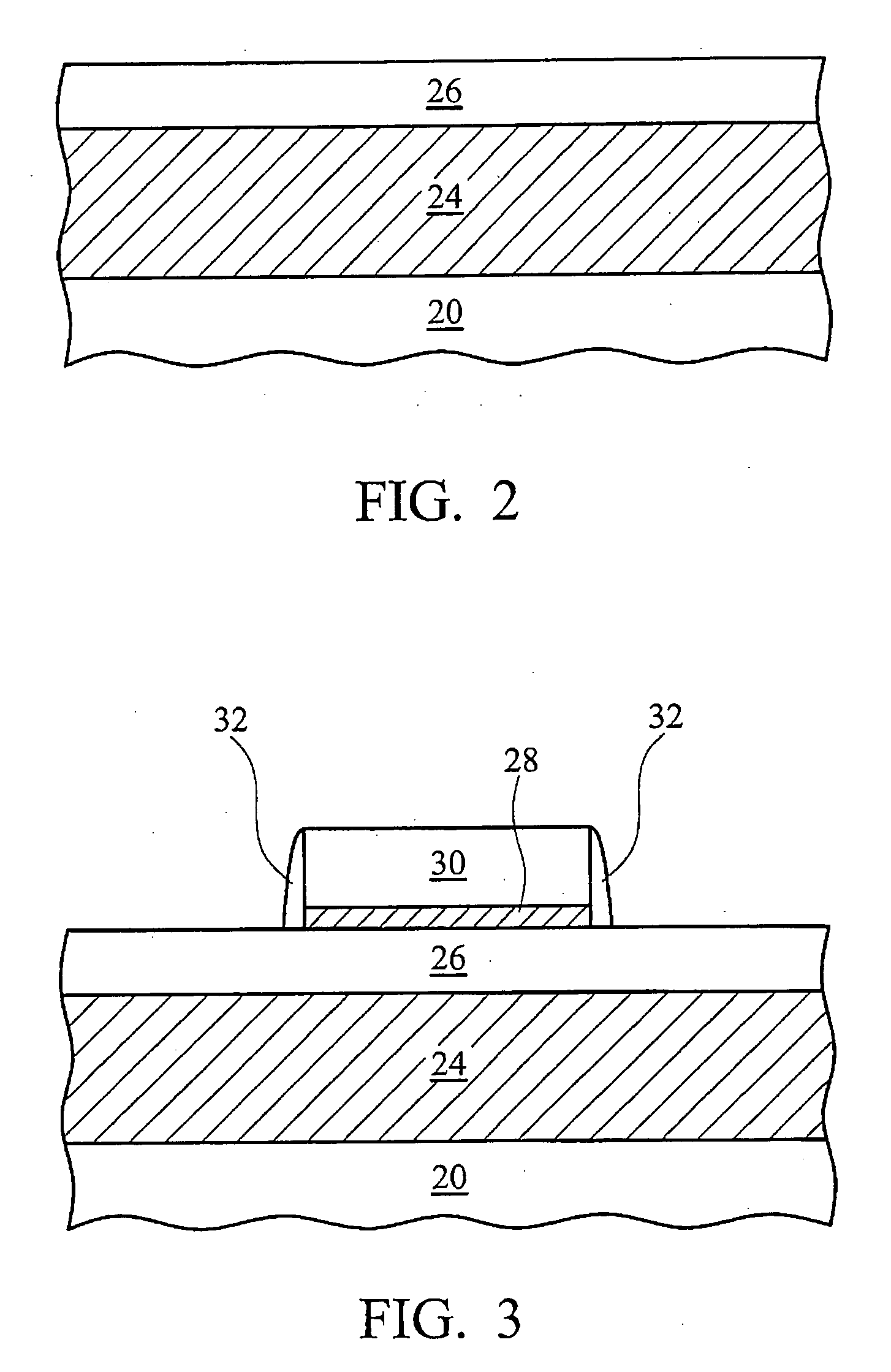
[0021] A novel structure having Schottky source / drain (S / D) and the method of forming such is presented. The intermediated stages of manufacturing a preferred embodiment of the present invention are illustrated. The variations and operation of the preferred embodiments are then discussed. Throughout the various views and illustrative embodiments of the present invention, like reference numbers are used to designate like elements.
[0022]FIGS. 2 through 5 illustrate intermediate steps in the manufacture of a preferred embodiment of a Schottky S / D DRAM of the present invention...
PUM
 Abstract
Description
Claims
Application Information