Atomic layer deposition apparatus

a technology of atomic layer and apparatus, which is applied in the direction of chemical vapor deposition coating, coating, metallic material coating process, etc., can solve the problems of unsuitable back end of line (beol) metallization process, inability to use multi-layer film deposition or graded film deposition, and inability to use in reaction chambers, etc., to achieve enhanced atomic layer deposition and broaden the choice of source chemicals

Inactive Publication Date: 2006-06-29
ASM GENITECH KOREA
View PDF5 Cites 371 Cited by
  • Summary
  • Abstract
  • Description
  • Claims
  • Application Information

AI Technical Summary

Benefits of technology

[0005] When the aforementioned ALD method is used, material is adsorbed on the surface of the substrate. A thin film is formed uniformly over the entire surface of a substrate regardless of the quantity of the process gas in each cycle because the amount of adsorbed molecules on the surface of a substrate is limited up to a maximum of a monolayer. Therefore, a uniform thickness of thin film can be formed even in the areas of high aspect ratio or large step difference, even when the thin film is formed with a thickness of several nanometers. Furthermore, the thickness of the thin film can be easily controlled by the number of process gas supply cycles, or ALD cycles, due to the self-saturating nature of the adsorption and the reactions.
[0006] Adding to the aforementioned advantages of ALD, we can get more useful benefits when a plasma is generated during the ALD cycles. For example, the use of plasma can help to broaden the choice of...

Problems solved by technology

This implies that one cannot use tantalum halides and H2 for ALD of Ta by the conventional thermal ALD at a temperature less than 400° C., making the process unsuitable for many back end of line (BEOL) metallization processes.
However, there is a limitation that it cannot be used for multi-layer film deposition or graded film deposition, which includes both PEALD and thermal ALD of a metallic film.
Once thermal ALD of metallic film is performed in the reaction chamber, PEALD is not possible in the reaction chamber before removing the metallic film due to shorting of the plasma-generating electrodes.
Any metallic film deposition due to thermal activation without plasma, whether during thermal ALD or PEALD, can coat insulator parts and electrically short the electrodes.
Although such a structural design can suppress the plasma generation above the showerhead, some risk remains for film deposition 16 on the surface of micro-feeding tube assembly 14 due to the thermal reaction.
If the deposited films 16 are electrically conductive, the electrical insulation between the showerhead assembly (26, 28) and the gas i...

Method used


Image

  • Atomic layer deposition apparatus
  • Atomic layer deposition apparatus
  • Atomic layer deposition apparatus

Examples


Embodiment Construction

[0061] Hereinafter, exemplary embodiments of the present invention will be described in detail with reference to the attached drawings such that the present invention can be easily put into practice by those skilled in the art. The present invention can be embodied in various forms, but is not limited to the embodiments described herein.

[0062] In the drawings, thicknesses are enlarged for the purpose of clearly illustrating layers and areas. In addition, like elements are denoted by like reference numerals in the whole specification.

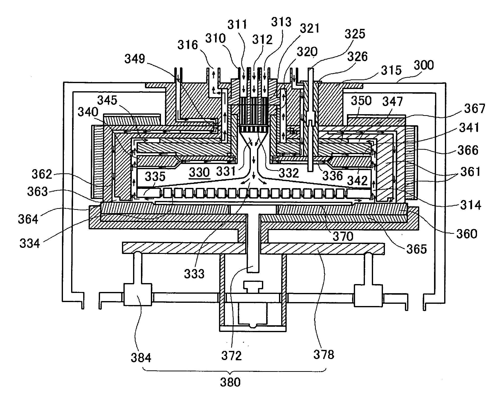
[0063] An ALD apparatus according to an embodiment of the present invention will be described in detail with reference to FIG. 4. FIG. 4 is a schematic cross sectional view showing an ALD apparatus according to an embodiment of the present invention.

[0064] Referring to FIG. 4, the ALD apparatus according to the embodiment of the present invention includes an outer apparatus wall 300, a gas manifold 315, a gas inflow tube 310, an electrically conductiv...


PUM

PropertyMeasurementUnit
Diameteraaaaaaaaaa
Diameteraaaaaaaaaa
Timeaaaaaaaaaa

Abstract

An atomic layer deposition (ALD) apparatus is, suitable for thermal ALD and plasma-enhanced ALD of conductive and non-conductive films. The ALD apparatus can maintain electrical insulation of a gas dispersion structure, such as a showerhead assembly, which acts as an RF electrode to generate plasma inside a reaction chamber while depositing electrically conductive films in the reaction chamber. Fine tubules of micro-feeding tube assembly prevents plasma generation in them and reactive gases each have separate flow paths through the micro-feeding tube assembly. Process gases out of the micro-feeding tube assembly enter narrow grooves of a helical flow inducing plate and form helical flows which mix well each other. Symmetrically mounted pads on showerhead assembly and flow guiding plate maintain a symmetrical gap through which an inert gas flows continuously to keep reactive gases outside the gap and unwanted film deposition in the gap. Longer operating time before maintenance (cleaning) and thus higher productivity can be achieved.

Description

REFERENCE TO RELATED APPLICATIONS [0001] This application claims the priority benefit under 35 U.S.C. §119(a) of Korean Application No. 10-2004-0113898, filed Dec. 28, 2004. This application is also related to U.S. utility application Ser. No. 10 / 486,311, filed Feb. 6, 2004, attorney docket no. ASMGEN.001APC.FIELD OF THE INVENTION [0002] The present invention relates to an atomic layer deposition apparatus capable of depositing a uniform thin film. In particular, the present invention relates to the reaction chamber structure of a plasma enhanced atomic layer deposition apparatus which is designed to prevent electrical short between plasma generating electrode and electrically grounded other parts, despite use of conductive elements during deposition. BACKGROUND AND SUMMARY OF THE INVENTION [0003] As semiconductor integration technologies advance, methods for depositing ultra thin films in a uniform and conformal manner, such as in a via or trench pattern, become increasingly import...

Claims


Application Information

Patent Timeline
IPC IPC(8): C23C16/00
CPCC23C16/14C23C16/45512C23C16/45536C23C16/45544C23C16/45565C23C16/45591C23C16/515
Inventor CHOI, SEUNG WOOLEE, CHUN SOOPARK, KWANG LAE
Owner ASM GENITECH KOREA
Why Eureka
Try Eureka